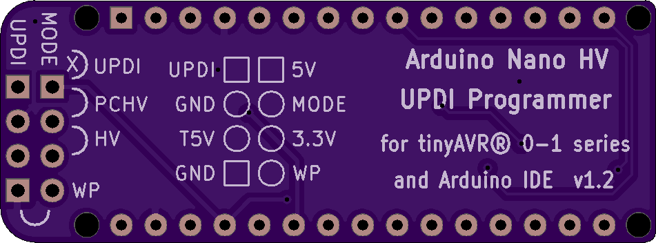
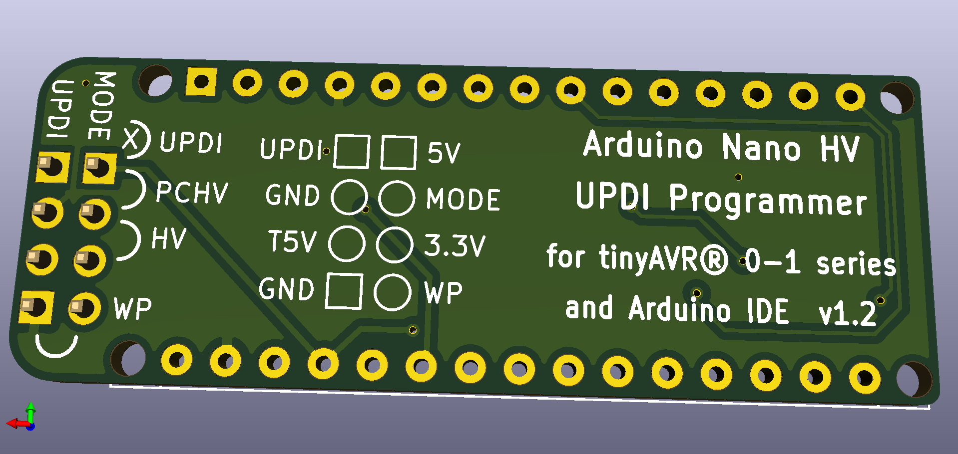
Arduino Nano HV UPDI Programmer
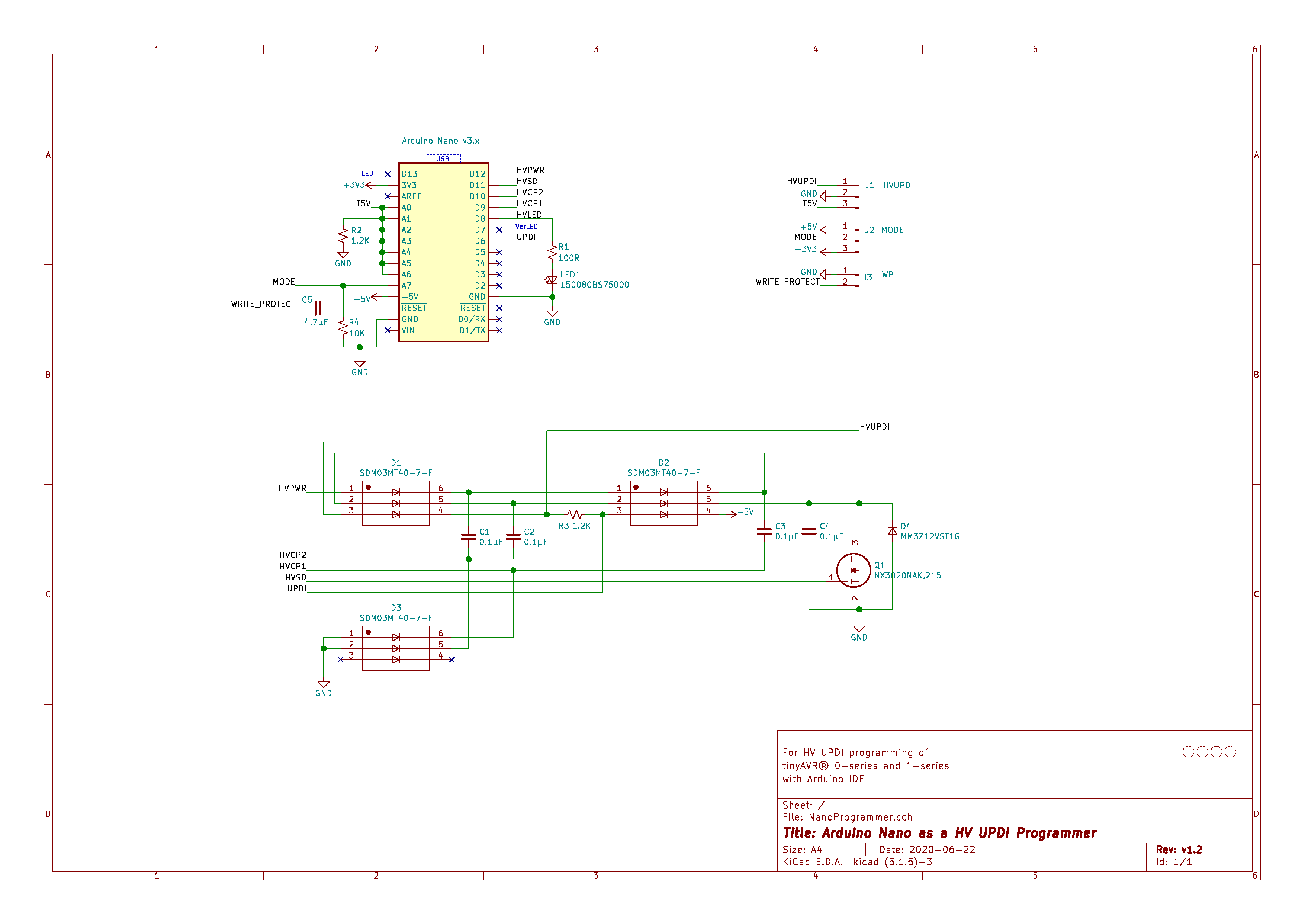
The Nano HV UPDI programmer will allow using the additional configuration settings for the UPDI pin without the fear of getting locked out from the MCU. There are 3 programming modes: UPDI, HV or PCHV (described below). The target voltage is 5V.
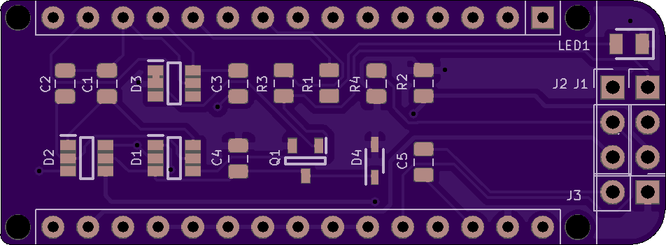
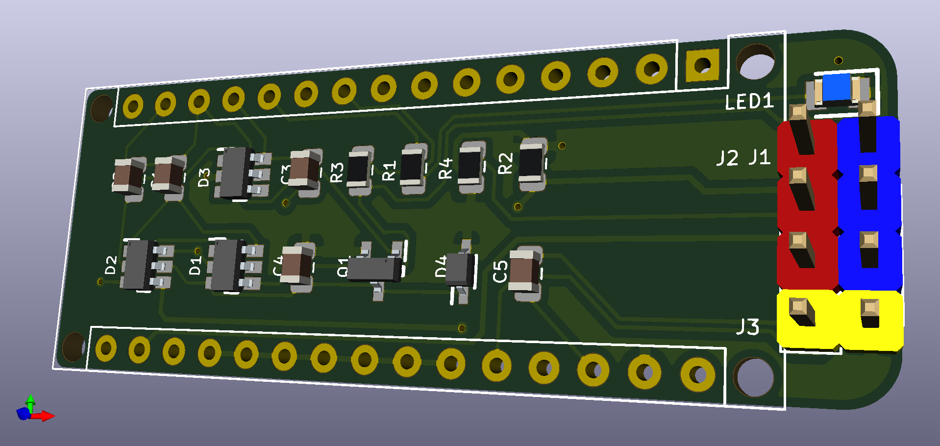
| Item | Qty | Reference | Part Number | Description |
|---|---|---|---|---|
| 1 | 1 | --- | PCB design OSHPARK | PCB shared design |
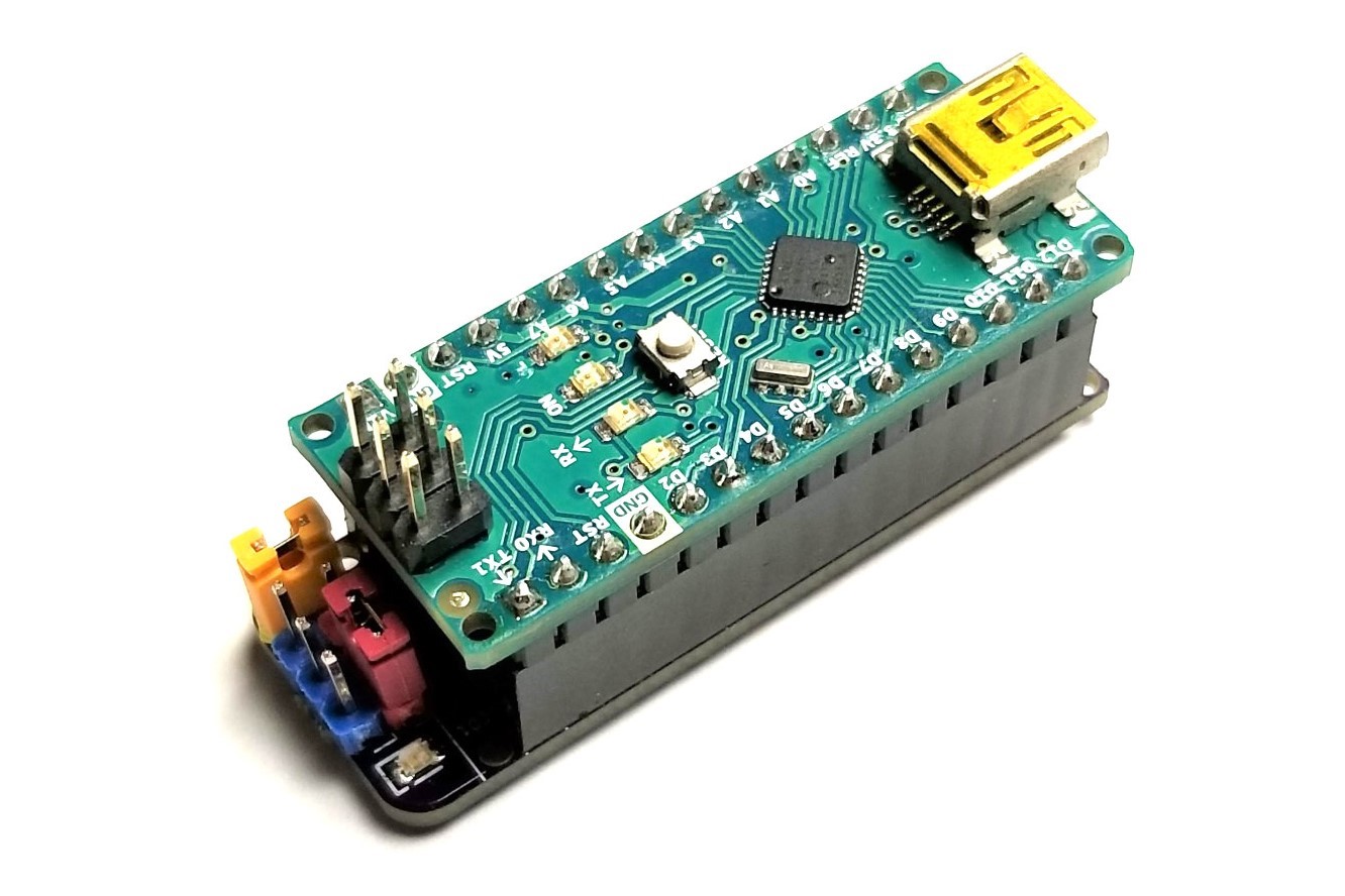
| 2 | 1 | --- | A000005 | Arduino Nano |
| 3 | 3 | D1, D2, D3 | SDM03MT40-7-F | DIODE ARRAY SCHOTTKY 40V SOT26 |
| 4 | 1 | D4 | MM3Z12VST1G | DIODE ZENER 12V 300MW SOD323 |
| 5 | 1 | LED1 | 150080BS75000 | LED BLUE CLEAR 0805 SMD |
| 6 | 1 | R4 | RC0805JR-0710KL | RES SMD 10K OHM 5% 1/8W 0805 |
| 7 | 2 | R2, R3 | RC0805JR-071K2L | RES SMD 1.2K OHM 5% 1/8W 0805 |
| 8 | 1 | R1 | RC0805JR-07100RL | RES SMD 100 OHM 5% 1/8W 0805 |
| 9 | 4 | C1, C2, C3, C4 | CL21B104KBFNNNG | CAP CER 0.1UF 50V X7R 0805 |
| 10 | 1 | C5 | CL21A475KAQNNNE | CAP CER 4.7UF 25V X5R 0805 |
| 11 | 1 | Q1 | NX3020NAK,215 | MOSFET NX3020NAK/TO-236AB |
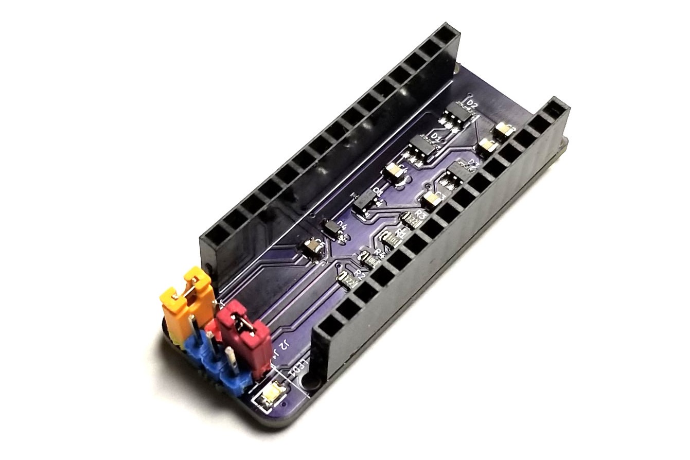
| 12 | 1 | J1 (UPDI) | --- | Pin strip male header, 2.54mm, 3-position, BLUE |
| 13 | 1 | J2 (MODE) | --- | Pin strip male header, 2.54mm, 3-position, RED |
| 14 | 1 | J3 (Write Protect) | --- | Pin strip male header, 2.54mm, 2-position, YELLOW |
| 15 | 2 | --- | --- | Female socket header, 2.54mm, 15-position |
-
Install megaTinyCore
-
Install the HV Programmer Firmware
● Click on the green "Clone or download" button, then select "Download ZIP".
● Unzip this file in a folder on your PC, then rename the jtag2updi-master folder to jtag2updi
● In the Arduino IDE, open the sketch "jtag2updi.ino"
● Remove the Write Protect jumper from the programmer.
● From the IDE, select Tools > Board > "Arduino Nano".
● Then select Tools > Port > (serial port used by the Nano).
● Then select Sketch > Upload.
● Install the Write Protect jumper.
-
From the IDE, select Tools > Programmer > "jtag2updi (megaTinyCore)".
You can now use the Nano HV programmer to "Burn Bootloader" or to "Upload Using Programmer" from the Arduino IDE. Make sure to choose the appropriate board, chip and port setting target.
Programmer Mode Selection:
| Jumper J2 | Prog Mode | PA0 Configurations | HV Pulse | Power Cycle |
|---|---|---|---|---|
| no jumper | UPDI | UPDI | NO | NO |
| pins 2-3 shorted | HV | UPDI, RESET | YES | NO |
| pins 1-2 shorted | PCHV | UPDI, RESET, GPIO | YES | YES |
Recommended Connections:
| Jumper J2 | Prog Mode | PA0 Configurations | 3-pin Header | 6-pin Header |
|---|---|---|---|---|
| no jumper | UPDI | UPDI | GND, UPDI | 5V |
| pins 2-3 shorted | HV | UPDI, RESET | GND, UPDI | 5V |
| pins 1-2 shorted | PCHV | UPDI, RESET, GPIO | T5V*, GND, UPDI | 5V* (see results below) |
Status Led Operation:
Red and yellow LEDs are ON when in programming mode. On startup, the yellow LED will indicate overload status. It also indicates a failed programming session if it remains on. When the programming mode is set to HV or PCHV, a bright blue LED will flash to show the HV pulse during programming of the target.
OVL Sense:
On startup, the OVL sense analog input (A6) will be checked. If the voltage on A0-A5 (target power) has dipped below 90% (4.5V), then the yellow LED will indicate overload status by blinking at 4Hz. The user will then need to correct the problem and press reset to clear.
Target Power:
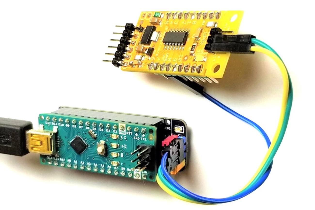
This is normally provided through the UPDI 3-pin header on the pin labelled T5V. The current limit is about 60mA and the voltage will normally be about 4.8V since its being sourced by PORTC on the programmer. If your target device requires more power, there's a 5V pin available in the 6-pin header. Using the 5V pin for power will only mean loss of the auto power-cycle feature, but this could easily be done manually.
Reset Button:
Resets the programmer and OVL status. It can also be used to provide a manual power-cycle to the target device when using the T5V pin.
UPDI Mode:
Used when the UPDI pin is configured as UPDI. Also used for any target device that isn't HV UPDI tolerant.
HV Mode:
Normally used when the UPDI pin is configured as reset. If used while the pin is configured as UPDI, it may require a second programming attempt for success.
This mode applies the 12V UPDI enable sequence (HV pulse) at power up and at the start of each programming sequence. This reconfigures the UPDI/Reset pin to UPDI mode which will remain in this state until the next POR. This allows programming to occur when the pin is configured as Reset or GPIO. A power on reset (POR) needs to occur for any fuse setting changes to take effect.
PCHV Mode:
Normally used when the UPDI pin is configured as reset or GPIO. If used while the pin is configured as UPDI, it may require a second programming attempt for success.
Power Cycle High Voltage mode (PCHV) will initiate a power cycle and HV pulse at the start of the programming sequence. At the end of the sequence, a second power cycle will occur which causes any new fuse setting to take effect. The power cycle OFF duration has been set to 115ms.
Write Protect (WP):
With jumper installed, the auto reset circuit of the programmer is disabled. This protects against accidental overwriting of the firmware and also ensures quick programming sessions by eliminating extra bootloader delays that would be caused by triggering the reset. Remove the jumper prior to updating the firmware.
Circuit Description (Dickson Charge Pump):
This is a 3-stage charge pump with MCU controlled voltage supply (HVPWR), shut down (HVSD) and two clocks (HVCP1 and HVCP2). The Schottky barrier diode arrays used have low capacitance, low forward voltage drop and low leakage so as not to effect the UPDI signal. Since there are 3 stages and 2 clock sources, the HVCP2 will see twice the capacitive load than HVCP1. This unbalance is compensated for by the unbalanced timing delays and pulse widths in the firmware which improves efficiency to the output. There is one MCU cycle dead-time between pulses and the charge pump clock frequency is about 413kHz with 16MHz CPU.
The HV pulse duration is about 700µs and has approximately 250µs exponential ramp-up to 12V. The 12V zener diode has a tight VZ tolerance, low capacitance and low leakage current. An N-channel MOSFET is used to quickly discharge the capacitors within 5µs, which is well within the 10µs allowed to release the HV pulse. The fast discharge drives a high energy negative pulse at each of the clock signals, so this is clamped to GND by several Schottky diodes to protect the MCU. A Schottky diode is added after the regulator to isolate the charge pump from the UDPI signal during normal UPDI transmission. The programmer's UPDI signal is protected from the 12V pulse by a series 1.2K resistor and a Schottky diode tied to 5V.
- Arduino 1.8.13
- megaTinyCore 2.1.5 via Boards Manager
- Chip Settings: Clock 20MHz, default timer, Support serial event: No, BOD 1.8V, BOD Mode: Disabled, EEPROM Retained, SUT 8ms
- ATtiny412F on SOIC-8 to DIP-8 adapter
- Programmer UPDI connected directly to target UPDI pin (PA0)
| Programmer Mode | UPDI Pin Mode | Optiboot Option | Target Power | Upload Using Programmer | Burn Bootloader |
|---|---|---|---|---|---|
| UPDI | UPDI | No | T5V | Success | Success |
| 5V | Success | Success | |||
| Yes | T5V | Success | Success | ||
| 5V | Success | Success | |||
| HV | Reset | No | T5V | Success 1 | Success 1 |
| 5V | Success 1 | Success 1 | |||
| Yes | T5V | Success | Success | ||
| 5V | Success | Success | |||
| PCHV | GPIO | No | T5V | Fail | Fail |
| 5V | Success 1 | Success 1 | |||
| Yes | T5V | Success | Success | ||
| 5V | Success | Success |
Success 1: Success or Fail toggles, may require 2 programming attempts
Fail: ...bad response to leave progmode command: RSP_NO_TARGET_POWER
Workaround: Use 5V power pin or switch jumper to HV mode (may require 2 programming attempts)