connections are not being followed through bus definitions across views #3678
Comments
|
For a simple demonstration of the working/not working GND ratsnest wire, take the previously uploaded .fzz file, unstack the shield, and on breadboard view connected a wire from the shield GND beside VIN to the same pin on the UNO. No ratsnest wire is shown in the schematic view.
Now move the wire to the next GND on the uno board in the breadboard view. A ratsnest wire shows up in schematic view. Though, based on the yellow highlights, those pins should be equivalent (in breadboard view).
|


|
I have a solution that mostly works for the use cases I know about. Instead of removing the view from the fzp connector definition, keep it as normal, but align the svg graphics exactly This may be the intended method. The file format information on the wiki does not SAY that the connector definitions must have an entry for every view, but it does not say they are optional either. Keeping that, and the associated element in the svg files, as required (at least when any connection on the same bus is being used in the view) gets the bus working correctly. That leaves the explicitly optional hybrid connectors as a possible method of hiding connectors in some view(s). I have not been able to get those to work as expected in combination with bus groups, and have not found an existing part where it does either. Any of the samples I looked at that use hybrid for a connector that is also part of a bus have various strange symptoms. I think bus connections should be followed whether the connectors have a graphical representation in the view or not. But this gives a way to make it work. Working example
The pcb view is still not working in this example. I have not added the pcb view of the uno connectors. |


Current BehaviourHere is a demonstration of the issue use simple standard core parts. Something a lot more convenient for debuging than the custom parts used above. The JST-VHR-3N connection part includes hybrid connectors on the pcb view. Wires added to those pins in the schematic view do not propagate (as ratsnest wires) to the PCB view, even though the hidden pin is included on a bus that another pin in the pcb view is on. Screenshots are from version 0.9.5 development build but exactly the same symptoms seen using 0.9.4b. The basic part layout, done in schematic view. The breadboard view showing ratsnest wires matching the schematic wires. Moving the parts on breadboard view gets the ratsnest wires to connect to either of the connectors on the bus. Whichever gives the shortest wire. The expected behaviour. PCB view though does not show the connection to the capacitor, which on the schematic view is connected to pin 6 (connector5), which is marked as a hybrid connector for the pcb view. Build: Version 0.9.5 (dCD-548-16-g6145d6d0 2020-04-19) 64 [Qt 5.12.7] Operating System: Fedora 31 (Workstation Edition) Steps to reproduce:
Expected BehaviourA ratsnest wire should shown on the PCB view from the capacitor to J1(3) |


|
Turns out that this is not really an application bug. More of a bug in the available documentation. After some additional experimentation with combinations of settings for part definitions and svg connector elements, I have a process that creates parts with hidden hybrid connectors in some views, while properly following related bus connections to generate the appropriate ratsnest wires when a connection is created in a different view. I have updated the hybrid section of the 2.1 Part file format wiki article with the results. Summary:
The core part used to demonstrate the problem is broken. It marks the hybrid connectors as being on the "unknown" layer. Changing that to "copper1", and moving the svg elements to that layer, got it to work properly. A bug report needed for the parts library, but not for the application. There is still one limitation left for this. If NO pins are to be displayed for a view, this correctly hides all of the connectors, but the empty (blank) part and its (not blank) part label are still shown. This could happen for an "inline" or "external" part, that does not normally have any representation on the pcb view, but is useful for breadboard and schematic. An application enhancement would be yo have a way (in parts definitions, or in inspector) to mark a part as only existing for specific views. Which would turn all connectors in that view to hybrid, AND hide the part itself. |
|
@mMerlin , from reading all the issue, it looks like this is not a bug. Do we need more tests? Do we need to improve the documentation? Can we improve the handling of hybrid connectors somehow in the application? Is just adding support for views where there are no connectors (and hide the part and part label)? Or should we close the issue? Notice that the oddities when displaying wrong info in the tooltip is bug #3578, which I think I manage to solve (#3973). |
|
Maybe the 'issue' is that the purpose of hybrid has not been described. When should it be used, and what functionality does it provide? My exploration says that it provides zero extra functionality. It still requires invisible connectors in the svg files. The only difference seems to be that (maybe) hybrid pins for a bus do not need to be stacked up. Other than the tooltip fix you mention. For other (non-bus) cases, what is the difference between hybrid and simply not including the connector for a view? This is not just views with no connectors. It is views with not all connectors that exist in other views. One example would be hats and shields that include prototyping areas. Those blocks of pins are typically not useful in schematic view, but can still want them in breadboard. Another case might be a module with a header that connects to pcb, but also has (on the reverse side) a header for configuration jumpers. Only the one header is wanted in pcb view. What is the 'correct' Fritzing implementation for those? My reading says that hybrid 'looks' right, but I don't see any advantage to using it over simply excluding the connectors from the view in the fzp. Other than FritzingCheckPart is likely going to complain about missing connectors. |
If you remove the connector from a view, I think it does not update the connections in other views in the view where the connector does not exist (even if there is a bus in other view). See https://forum.fritzing.org/t/suggestions-for-additional-documentation/15135/19 I guess that we really want is that an hybrid connector does not need any connector in the svg file or layer. Additionally, another tag (e.g., severalPins="yes") could be used for specifying that a connector represent that connector and all the connectors in the bus that are hybrid. This tag must only appear once for each view and bus. Thus, when you hover the mouse over the connector could say something like "wiper (2, 4)" where the numbers represent the all the numbers of the connectors that are hybrid and in a bus and the non-hybrid connector. I think that with these two features we could reuse svg files for different parts. For example, one SMD part and a THT part could share the same schematic symbol even if they differ in its pin count. |
Current Behaviour
The setup:
The (custom)
arduino_uno_for_shieldspart has multiple bus definitions. Among them are entries to connect the digital IO pins D11, D12, D13 to the ICSP1 header pins for MOSI, MISO, and SCK. The part contains connector definitions for all of those pins, but the ICSP pins deliberately do not includeschematicViewentries. Since they are bused together, and schematic view is a logical view, any connection (on any view) to D11, D12, D13 should also be a connection to the matching ICSP1 header pins. More on should in a moment.The
dragino_lora_shieldpart also includes multiple bus definitions. Here, the ICSP pins are NOT linked with the digital IO pins. However, both the ICSP header and associated digital IO pins ARE bused to pins on a configuration header.Another bus definition in the uno part, is for the 5 ground pins. 4 of those pins exist on the shield (there is no ICSP2 header here), but they are left as individual pins, not grouped together by a bus definition.
Holding mouse down on the bused pins of the individual parts in breadboard view shows the pin, and each of the bused pins, as yellow. In the current implementation, the pcb view for the uno is blank, but the shield exists, and the bused pins light up with mouse down on one of them. The schematic view has definitions for both parts, but currently none of the bused pins have more than a single representation, so individual part buses are not readily visible here.
When the shield board is dragged over the uno part in breadboard view, the matching pins turn blue, showing a valid connection. When (aligned correctly and) released, those shield pins turn green, plus the extra header pins that are (both) bused within the shield part and are (now) connected to one of the uno pins. That is the configuration header pins that are bused to the digital IO or ICSP(1) header pins. In addition, the Arduino digital IO side of the enable jumper headers light up. The shield side of those jumpers stay red, but mouse down on them turns the bused shield digital IO pins yellow.
With the shield
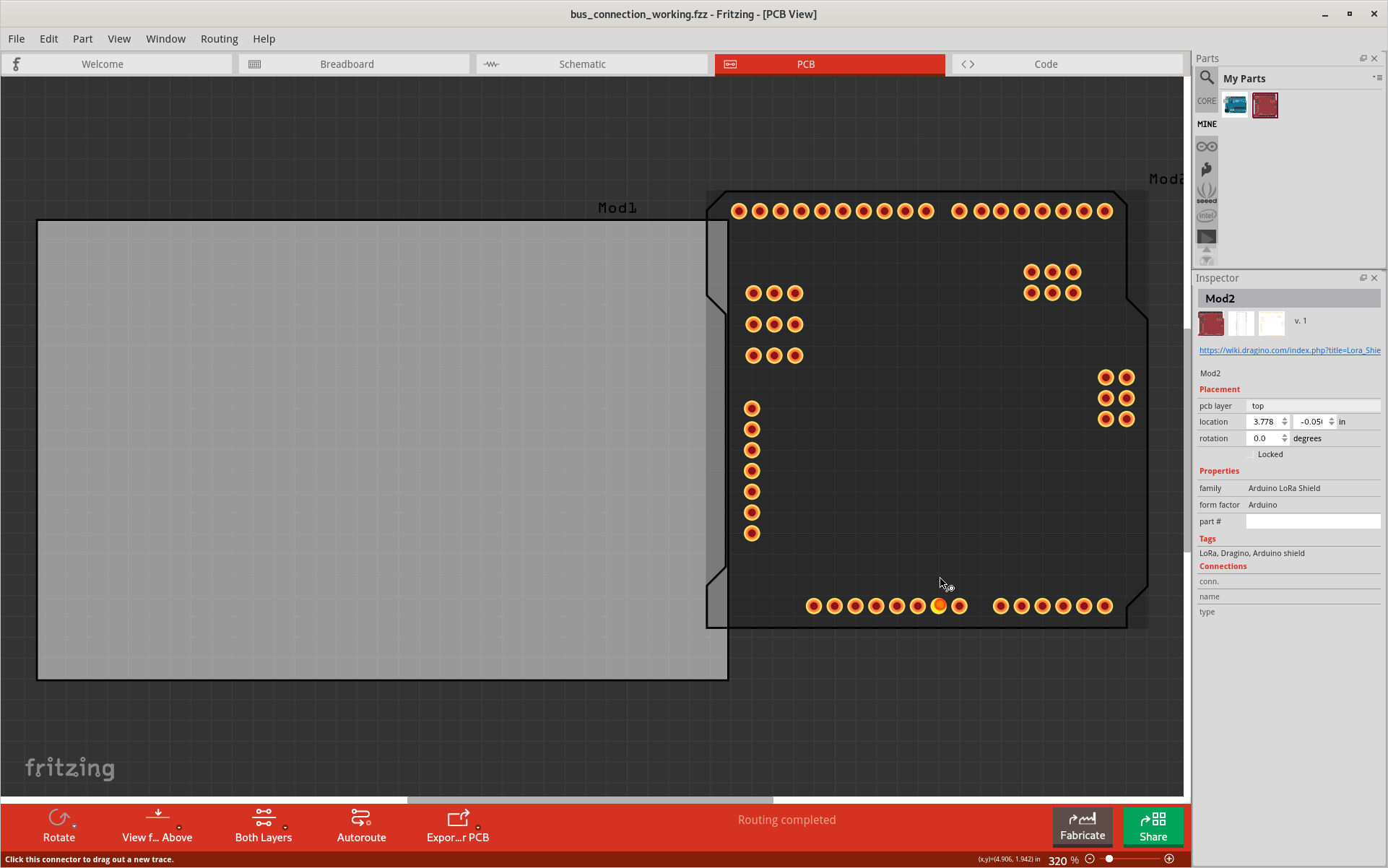
mountedon the uno, mouse down on any of the bused connections turns the whole group yellow. Of note here are the ICSP(1), configuration header, and Arduino digital IO pins. Mouse down on (for example) D13 turns D13, ICSP1 SCK, SV2 pin 1, and SV2 pin 3 yellow. The uno part has D13 bused to ICSP1 SCK, the shield part has D13 bused to SV2 pin 3, and ICSP SCK bused to SV2 pin 1. With the shield part aligned/connected with the uno part, the 2 D13 pins are connected, and the 2 ICSP SCK pins are connected. So all 6 of the pins are connected. In breadboard view, they actually show as connected using mouse down on one of them.All of that looks correct, but PCB view does not show quite the same information. There are no uno connection pins to click on, but the pins for the shield are available. Mouse down on D13 here turns only it and SV2 pin 3 yellow. The connection to ICSP SCK, via the shield to uno D13 connection, uno bus from D13 to ICSP1 SCK, uno ICSP1 SCK to shield ICSP SCK is not seen, nor the extension of that to SV2 pin 1 through the bus on the shield. A simpler failure is the ground connections. Each of the 4 GND pins on the shield is connected to the matching GND pin on the uno, and all of the uno GND pins are grouped in a single bus. However, mouse down on the pcb view shield GND pins does not show any of the others as connected.
The schematic view has issues as well. The GND pins of the uno and shield are not shown as connected. The 3V3 and 5V pins are connected, as shown by the ratsnest lines. The 3V3 is easy. There is only a single 3V3 pin on each of the uno and shield parts, and they are connected by the placement of the shield part on the uno in the breadboard view. The 5V is a bit more complex. There are 3 5V pins on the uno part grouped into a bus. Each of the 2 5V pins on the shield is connected to a matching 5V pin on the uno by the shield placement in breadboard view, plus the single schematic view 5V pin for each part is matched to the main 5V pin. The 2 5V schematic pins are hooked to connections that are directly connected in breadboard view. Like the 3V3 connection, no bus needs to be referenced to show the linkage.
As described above, the 5 uno part GND pins are grouped into a bus, but the 4 shield part GND pins are left separate. For the schematic view shield part, the single GND pin is associated with the GND pin that is beside (in breadboard view) VIN. The single uno part schematic view GND pin is associated with the second power header gnd pin, which is beside (in breadboard view) 5V. In schematic view they are not connected. No ratsnest line, and nothing else turns yellow with mouse down on the pins.
As shown on breadboard view, the 4 ICSP SCK pins are connected and grouped together. On schematic view, that is not visible. Mouse down on one of the D13 pins only turns it and the other D13 pin yellow. Mouse down on the shield ICSP SCK pin only turns it yellow.
The fact that the 2 physical pins are tied together, as defined by the bus definition, is not being seen as creating a connection between the GND pins in schematic view. Same for PCB view. The connections are not being followed from PCB view pin, to connected part pin, through connected part bus, back to another pin on PCB view. The schematic view case is simpler, since there is at least a GND pin from the bused group in the view, even it is not the one that is directly connected in the breadboard view. The pcb view does not have a GND (or any) pin for the uno. But in both cases, the internal connectivity information should be providing a path through the physically connected pins, and the bused pins that are grouped with them.
Here is the sketch with custom parts that were used to generate the screenshot images. Remove the trailing .zip to open it.
bus_connection_ignored.fzz.zip
Build:
Version 0.9.5 (dCD-548-17-g694c4a08 2020-04-27) 64 [Qt 5.12.7]
Same symptoms with Fritzing 0.9.4.2019-12-01.CD-498
Operating System:
Fedora 31 Workstation
5.6.11-200.fc31.x86_64
Steps to reproduce:
Expected Behaviour
Every view should use the part bus definition information, and connections to the associated pins (in any view) when checking what should be connected by ratsnest or shown as connected on mouse down.
The schematic should show a ratsnets wire between the part GND pins
Mouse down on either GND in schematic view show show the other GND as connected
Mouse down on Either D13 or SCK in schematic view should show all 3 pins as connected
Mouse down on any of the shield GND pins in PCB view should show all 4 as connected
Mouse down on any of D13, SV2.1, SV2.3, ICSP SCK of shield part in PCB view should show all of them as connected
The GND pins in schematic
The text was updated successfully, but these errors were encountered: