eSim
skywater130 pdk
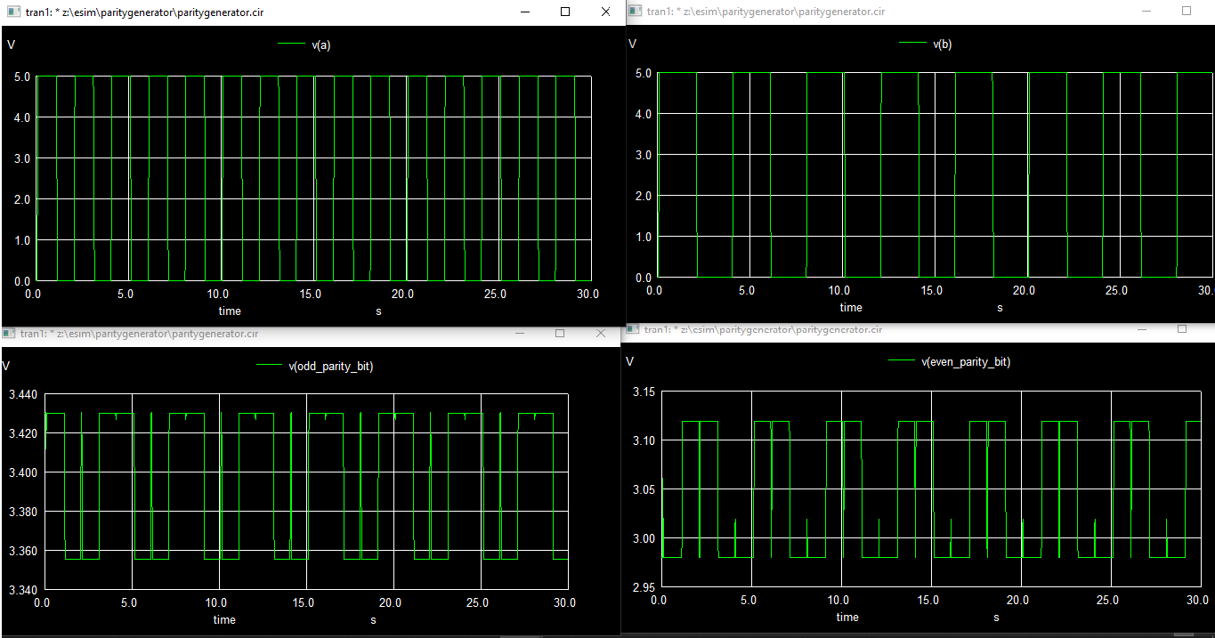
Parity generator is a combination logic circuit. When data is transmitted between source and destination there should not be any loss in data. To detect data losses parity generator technique is used in transmitter end. Parity is the extra bit added to digital data on transmission. There are two types of parity generator even parity generator and odd parity generator.Even parity generator look for even number of ones in binary data here parity bit is one when it detect odd number of ones else it is zero. Odd parity look for odd number of ones in binary data here parity bit is one when it detect even number of ones else zero.
Pseudo NMOS logic is a type of static cmos logic where complementary output is driven between Vdd and ground. This complementary output can be normalized by cascading an inverter to it. In this logic the number of transistors required is N plus 1 where N is the number of inputs. A complete logical expression is implemented using NMOS transistors with one PMOS transistor which is grounded . Vdd is given to the source terminal in pmos. As this logic is more prone to static power decipation to avoide this size of pmos will be made smaller than nmos.
While the SKY130 process node and the PDK from which this open source release was derived have been used to create many designs that have been successfully manufactured commercially in significant quantities, the open source PDK is not intended to be used for production settings at this current time. It should be usable for doing test chips and initial design verification.
2 bit even and odd parity generator is constructed by cascading 2 Exclusive OR or XOR gates. XOR gate gets 2 inputs and leaves an output. In XOR gate output will be true or high only when there is an odd number of one is given as input and output will be false or zero when even number of one is given as input. XOR gate implemented using pseudo NMOS logic. In this design we have taken two inputs A and B with one output PARITY BIT. The type of parity generator is choosen by baising Dc source at pin 5 and pin 7. If DCunderscoreB is high odd parity is generated. If DCunderscoreB is low then even parity is generated. Odd parity denotes ODD PARITY BIT and even parity denotes EVEN PARITY BIT. Expression for ODD PARITY BIT is equal to ~(A^B). Expression for EVEN PARITY BIT is equal to A^B. Pin 1 is A Pin 2 is D which is B bar pin 3 is C which is Abar pin 4 is B pin 5 is DCunderscoreD pin 6 is vdd pin 7 is DCunderscoreB and pin 8 is PARITY BIT. We can get output plot from 8th pin.