This is an implementation of the paper: https://arxiv.org/pdf/1901.08204.pdf
The paper proposes a method to first detect PCB defects using template matching and image processing. Then classify each of the defects using a Densely Connected Convolutional Network (DenseNets) into the following categories,
- Missing Hole
- Mouse Bite
- Open Circuit
- Short
- Spur
- Spurious Copper

The DenseNet has a very popular structure with local interconnections as shown below

In the model proposed, two of these "dense" blocks used are encapsulated between Covolution and Pooling layers as shown below

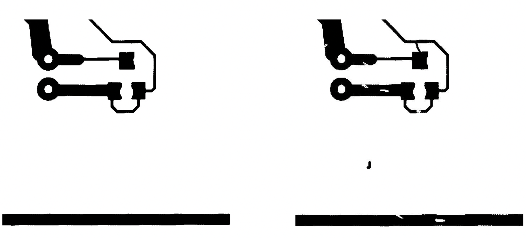
A sample template (left) and defective image (right) are shown below
From here, after template matching and some image transformations (detailed in the paper) we localize the defects as shown

Feeding an ROI drawn around each of these defects to the DenseNet, the final result has the defect labelled along with the confidence
