Our stm32 documents
Clock diagrams:
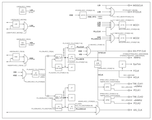
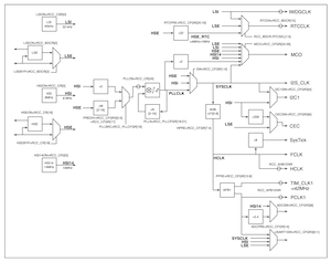
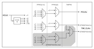
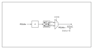
We found the clock tree figures very confusing (e.g. Figure 13 in DM00031020 ). So are the paragraphs on the TIM_CLKs and TIMPRE. The following figures are our versions that combine various pieces of information from the datasheets, and experiments we did on the DISCOVERY and AshimaCore boards. The clocktree*.xml files in the library are written against these diagrams.
Peripheral Arrangement
The datasheets are messy about how they name various areas and busses. For example the AHB1 bus has two peripheral bridges and various directly connected peripherals. The datasheet, registers and other documentation (mostly) start the 'AHB1' bus after the two peripheral bridges, with offsets of zero; when it seems better to treat the bridges as the first two peripherals on the AHB1 bus. Additionally the ADC, DMA, USB, and Ethernet devices are better described as bridges with sub peripherals.
To fix this I added a layer to the memory hierarchy called 'Bus1', 'Bus2' etc, from which the APBx AHB1 Eth and ADC are bridged.
When organized like this the offset block number (sector) lines up precisely with the enable register bit locations; giving me some confidence that this organization more closely resembles how ST designed the underlying structure of the chip. Could be wrong though!!
Bit Banding
The Datasheet is a little unclear on how bit banding is done. It suggests banding is done only for blocks 1 and 2, and the cortex-M3 documentation concures and sais these blocks are 1MB long. so:
Block 1 : 0x20000000-0x200fffff maps to 0x22000000-0x23ffffff
Block 2 : 0x40000000-0x400fffff maps to 0x42000000-0x43ffffff
Note :
-
In the Standard Peripherals Library from ST; stm32f40xx.h gets the bit banding WRONG.
-
CCM is not bit banded (The data sheet is INCORRECT in saying all SRAM is bit banded). (verified)
-
Offsets for SRAM and APB1 APB2 AHB1, etc must all be multiplied by 32! (verified) (SPL from ST has the offsets identical)
SRAM enable
The datasheet misplaces the enable bit for backup sram in the APB1ENR register instead of AHB1ENR (verified)


