SVG-PCB is…a browser-based, parametric Printed Circuit Board (PCB) design app.
Using a combination of Javascript code and graphical drawing tools, circuit board designs can be drawn and exported as a SVG, PNG file for production (etching, masking, milling, etc) as well as a JS code file.
SVG-PCB’s functionality is similar to other PCB design, formally called Electronic Design Automation (EDA), software such as Eagle, KiCAD or EasyEDA. While similar in ultimate functionality, SVG-PCB has some significant differences from those traditional PCB EDAs, including…
- No Schematic diagram creation
- No Ratsnest feature
- No Electrical Rules Check
- No Design Rules Check
- No Auto-routing
- Does not require installation...is browser-based
And of course the most notable difference is that SVG-PCB is an EDA that is centered upon Javascript programming...while having some very useful graphical user interface (GUI) features to make for a unique circuit board design experience.
Disclaimer: While SVG-PCB is easy to use, it is best suited for those with some knowledge and experience with PCB design…who are able to select, place and connect electronic components in a sensible and functional manner to make a working circuit...as well as some level of comfort with all aspects of programming, particularly Javascript.
SVG-PCB is a non-tradional EDA for those who enjoy the logical structure and parametric control...of Drawing with Code.
-
To access SVG-PCB go to https://leomcelroy.com/svg-pcb-website/#/home
-
On the HOME screen…you are giving 4 sub-page options
-

- Choose Editor > to enter the board design workspace

Let's take a tour around the SVG-PCB Board Design interface!
-
Right side >> Drawing Window
-
Left side >> Coding Window
-
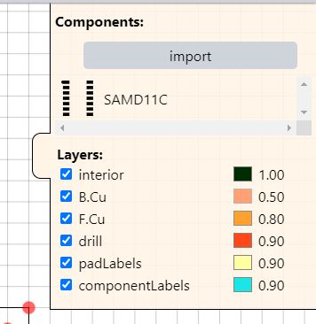
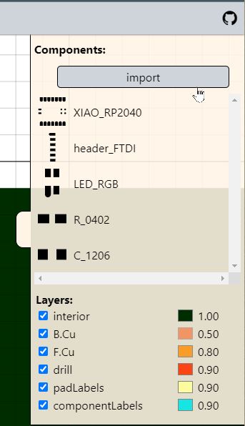
Components >> a Pop Out pane in the Drawing Window with options to…
- Import component footprint
- Make Visible/Invisible (checkbox) and change colors for board Layers
-
Top left side >> Menu

- Run (SHIFT + ENTER) >> runs the program…updates the image in the Drawing Window with changes to the code
- Be careful NOT to click NEW when test running your code...or you will erase all your progress! Save often!
- New >> opens a new program
- To Open Existing SVG-PCB file >> Drag & Drop a SVG-PCB .js file into the SVG-PCB browser window
- Download >> Export a file
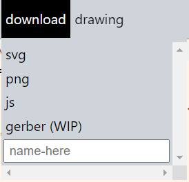 - Choose from **SVG**, **PNG**, **JS** file formats (**GERBER** a 'work in progress' feature) - Enter the unique **file name** in the “name-here” input box - **Note:** all exports saved to the **downloads** folder-
Center View >> centers the PCB board design in the Drawing Window…zooming to fit
-
Options >> toggle options for the Drawing Window

- Shapes and component control handles Visible/Invisible
- Grid and snap-to-grid ON/OFF gr
- Adaptive Grid ON/OFF
- SnapPad ON/OFF
- Grid Size define
- Vim Mode ON/OFF
- Run (SHIFT + ENTER) >> runs the program…updates the image in the Drawing Window with changes to the code
SVG-PCB’s design worksflow involves 4 procedures…
- Importing component footprints
- Adjusting the PCB shape and size
- Placing components on the PCB
- Routing wire paths between component footprint pads
The SVG-PCB design process will require a combination of selecting and positioning SVG graphic elements in the right Drawing Window of the interface and adjusting or writing code in the left Coding Window.
- From the COMPONENTS pop-out menu (Top-Right of the Drawing Window)…use the IMPORT button to find/select component footprints for your board from the COMPONENT MENU list

- Click once on the desired component to add it to the component footprint list
Tip: use the SEARCH bar to narrow your component search Tip: Resistor 1206 size >> discretes/R_1206.json Tip: Capacitor 1206 size >> discretes/C_1206
Note: Descriptive code for imported component footprints will simultaneously appear near the top of the Code Window…under the DECLARE COMPONENTS section as a Constant Variable (const)
Ex: LED 1206
const LED_1206 = {"A":{"shape":"M -0.037,0.034L 0.027,0.034L 0.027,-0.034L -0037,-0.034L -0.037,0.034",
                       "pos":[-0.055,0],
                       "layers":["F.Cu"],
                       "index":1},
                  "C":{"shape":"M -0.027,0.034L 0.037,0.034L 0.037,-0.034L -0027,-0.034L -0.027,0.034",
                       "pos":[0.055,0],
                       "layers":["F.Cu"],
                       "index":2}}
-
To DELETE unwanted component footprints
- In the Code Window…select the descriptive code of the unwanted component from within the DECLARE COMPONENTS section...press the DELETE key on the keyboard
Tip: Triple-click on a code line to select all the code on that line
Note: the component properties listed in the DECLARE COMPONENTS code section (such as the pad name or layer) can be edited. But do so thoughtfully!
Note: The COMPONENTS pop-up menu can be hidden away when not in needed…by clicking on the tab.
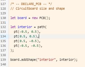
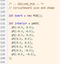
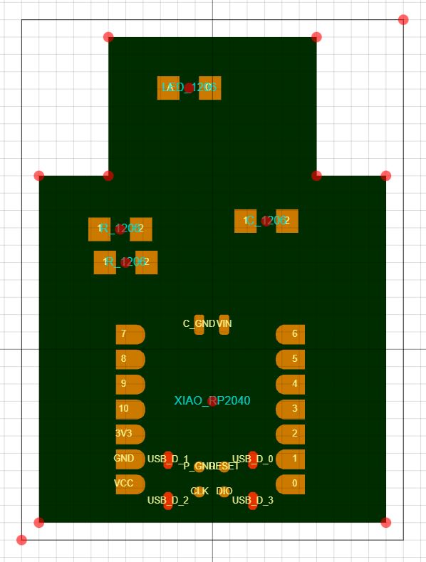
- The board Size & Shape is defined within the DECLARE PCB code section
- Add/Remove Points (pt) from the interior variable to change the shape of the board
- The board shape and size can also be changed by dragging RED Handles at the vertices of the board shape…or more precisely by adjusting the point’s values in the code
Original Shape

Adjusted Shape
- From the COMPONENTS pop-out window’s FOOTPRINTS list…Drag & Drop the graphical icon component to the board area
- Grab the RED component 'handle' to Move the component...and place it on the board
Note: After dropping a component onto the board area…code for the dropped component will appear in the ADD COMPONENT section of the code
-
ROTATE the component by changing the ‘rotate:’ value of the component’s code
-
Adjust the component’s displayed name and value by editing the ‘name:’ property
- ex: “R_1206” > “R1 100k”
- ex: “C_1206” > “C1 100uF”
KEY Tip: make each component into a ‘const’ variable with a short and simple name, such as “xiao”, “C1”, etc. Doing this will make WIRING in the next step much more efficient.
```
const SAMD =  board.add(SAMD11C, { translate: pt(-0.03, 0.01, rotate: 0, name: "SAMD11C" })
```
Tip: List the added components from top to bottom…with components whose position will be dependent on another component below the component it references.

This is where SVG-PCB departs from the methodologies of other EDAs. Instead of utilizing a GUI to parametrically arrange components on the PCB, SVG-PCB uses Javascript code to do the same. While it may feel a bit unintuitive at difficult at first, the logic and rationale of this method...along with some its advantages...will make itself clear over time. With that said...let's WIRE!
Key Note: Wiring between component pads in SVG-PCB is done most efficiently in the Coding Window in the ADD WIRES code section…using the Const Variable Name created in the ADD COMPONENT section.
SVG-PCB Wiring Procedure Overview
- Roughly position components on the board first…before Wiring…start with the major components (these will be the positional 'reference' components for other components' relative positions)
- In its simplest form, SVG-PCB WIRING requires specification of a Start-Point Pad from one component (the Reference Component) and an End-Point Pad from a second component (the Dependent Component)
- Intermediate Points are added in between the Start and End points...as required or desired...to shape the line
- All Pads and Points drawn in SVG-PCB are drawn on a Cartesian Coordinate System...and have X and Y coordinates associated with them
- Because SVG-PCB board designs are described by Javascript codes...the numbers representing the XY coordinates can be substituted by Variable Descriptors
Let's take a look at an example...
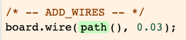
This is the generic code to create a WIRE…
board.wire(path(), 0.03)- The ‘board.wire’ command takes two parameters…line path, wire width
- 0.03mm is the default wire width
Tip: You might want to create variables in the 'Constants' section of the program (near the top) to represent different types of wire widths on your board...ex: const pwrWire = 0.04, const signalWire = 0.02
-
In between the parenthesis following the ‘path’ command…you will specify the starting point, intermediate point(s) and end point of the line.
-
These POINTs (RED dots) for a polyline will be specified using the pt(x-coordinate, y-coordinate) command
-
To make it possible to draw a polyline WIRE graphically in the Drawing Window…
- Click on
pathwhich should appear in green.
- In the Drawing Window…click on the locations of the start, intermediates and end POINTs

- Click on
-
For example…
board.wire(path(
  pt(-0.100, 0.100),
  pt(-0.2, 0.1),
  pt(-0.25, 0.400),), 0.03);
But the BEST way to create WIRE connections between two components…is to specify a pad from one component as the starting point, a pad from another component as the end point, and points in between (as required)
- The pads of every component has a unique number or name
By using Pad Names in combination with the Const Variable Name assigned to components in the previous step…explicit and fixed connections between 2 components can be specified
-
Pad Names + Const Variable Component Names can also be used as Reference Coordinates to position Intermediate Points
ex: Utilize the X-coordinate of one pad and the Y-coordinate of the other pad
-
The syntax for referencing a component’s pad name is...
- the component’s variable name +
- . +
- the word “pad” +
- the name of the pad in parenthesis and surrounded by quotes
-
Ex: To specify the “GND” pad for the “SAMD11C” component, you would write…
SAMD.pad("GND")- Pad Names can also be used as Reference Coordinates for a WIRE vertex point ****to align with…by using padX and .padY…instead of just .pad
- Ex: To specify the Y-coordinate of the “GND” pad for the “SAMD11C” component as a reference point, you would write…
SAMD.padY("GND)- Ex: To create a 3-point for a wire between the SAMD “GND” pad and the R1 “1” pad, you may write something like this..
- SAMD “GND”…as the starting point
- R1 “1”…as the end point
- ..and an intermediate point that references the SAMD “GND” pad’s y-coordinate and R1 “1” pad’s x-coordinate
board.wire(path(SAMD.pad("GND"), //starting point, GND pad of SAMD11C
               pt(R1.padX("1"), SAMD.padY("GND")), //Intermediate point referencing the X-position of the resistor pad 1 and Y-position of the SAMD GND pad
               R1.pad("1")), signalWire); //end point, resistor 1 pad 1 & wire width of 0.02, the signal wire type
Note: Pad Names can be edited or changed in the component description in the DECLARE COMPONENTS section (but do this with great care!)