This document is a guide for soldering a minimal build of the MiniF4 36-key split keyboard.
A companion video showing the soldering can be found here:
- Minimal:
- This build can be completed with a minimum of parts.
- Only a minimal soldering set required.
- Only simple soldering. No prior soldering experience.
- Since it does not involve diodes, there are fewer things which can go wrong.
-
This keyboard has only 36 keys.
- This can take some time to get used to.
- May not be ideal for tasks which involve use of mouse-and-keyboard.
-
This is a minimal, budget-oriented build.
- The keyboard is just the PCB and some switches.
- No plate/case.
- The resulting build doesn't feel as nice as if it were built with a plate or a case.
Other budget-oriented ways to build a keyboard:
The steps in this build guide will more/less apply to other keyboard PCB designs.
Other keyboard PCBs will be similarly cheap to fabricate/assemble if the PCB is also smaller than 100x100mm.
The most common development board used in such keyboards is the Pro Micro, which isn't as powerful as the WeAct Studio MiniF4 "black pill". There are development boards which are compatible with the Pro Micro while being more powerful, but these are more expensive. (Otherwise everyone would just use those in their builds).
It's likely to be cheaper to build a hand-wired keyboard.
This would involve getting a case by lasercutting plates, and hand-wiring the switches to the microcontroller development board.
The advantage to building a hand-wired keyboard is you've got more flexibility in terms of keyboard shape/size.
Compared to the build in this guide, the disadvantage to the hand wired keyboard is that it requires more fiddling with wires, and the result might not look as nice despite taking more effort.
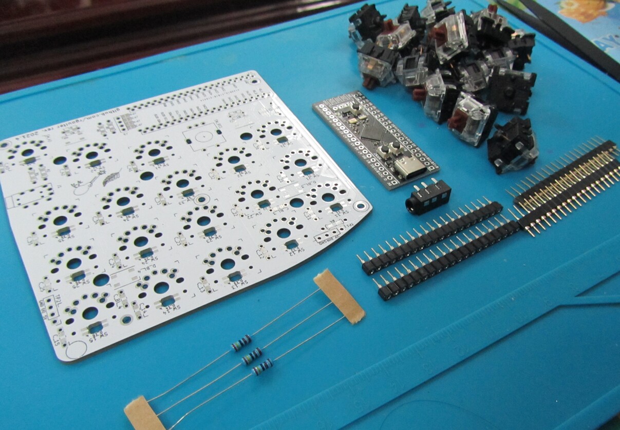
- 2x PCBs
- 6x 2.4k Ohm 1/4W through-hole resistors
- 2x PJ-320A TRRS jack
- 2x WeAct Studio MiniF4 "Black Pill" development boards
- WeAct Studio endorsed links can be found on their repository's README
- 2x 1x40 SIP round female header sockets or 2x DIP40 round pin socket and 2x 1x40 SIP round male header sockets
- 36x MX-compatible switches
- 36x keycaps, compatible with the MX switches
- 10x Bumpons, 5mm x 2mm.
- 1x TRRS cable
- 1x USB-C cable
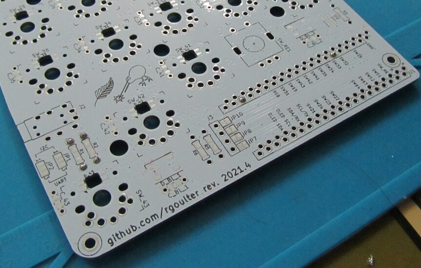
The round SIP headers are for socketing the development board. i.e. making it so that it's easy to remove and replace the development board.
Using DIP40 sockets instead of SIP 1x20 female headers makes it somewhat easier to assemble.
Instead of the round male header pins, it is also possible to socket the development board using tinned wire (e.g. stripping wrapping wire). This results in the development board sitting lower, but requires more effort than just using the male header pins.
If you're confident, then you could directly solder the development board using the male headers provided with the development board, rather than socketing.
It's also useful to have:
- ST-Link v2 STM32 programmer.
- The STM32F4 comes with a DFU bootloader. i.e. In theory, the STM32F4 board can be flashed without needing the ST-Link. In my experience, this can be finicky and unreliable; so I recommend using an ST-Link. The cheap knock-offs work.
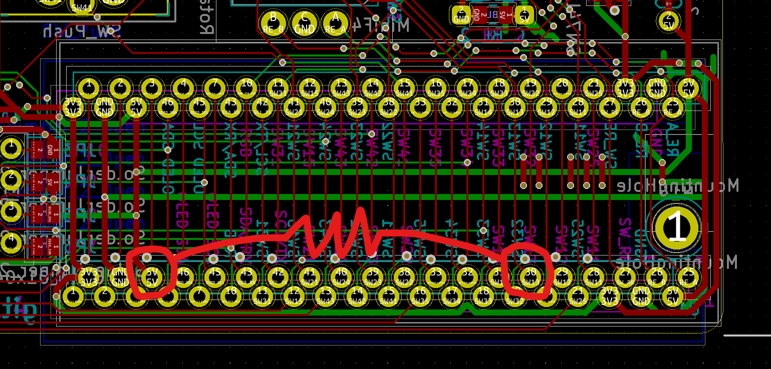
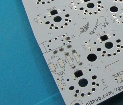
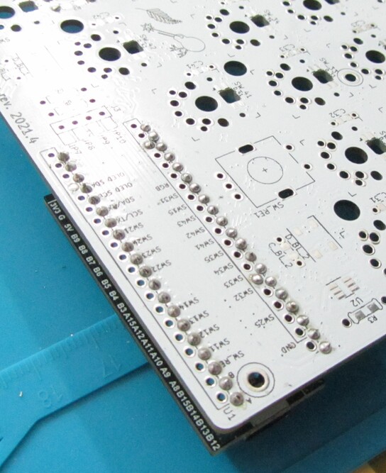
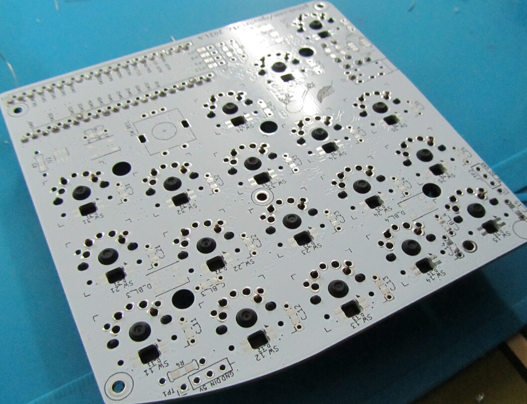
- Solder the resistors at R1, R2.
- Solder one of the resistors from PA9 (labelled SW13) to 5V or 3V3.
- It's more convenient to use the plated through hole pads for the 'reverse' side of the board.
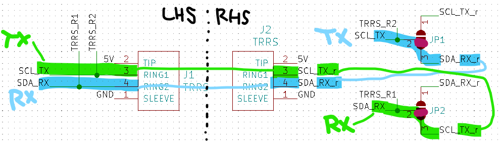
- For the Right-Hand Side, solder jumpers JP1, JP2.
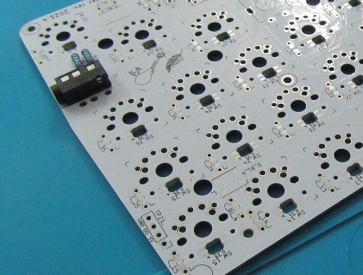
- Solder the TRRS jack at J1/J2.
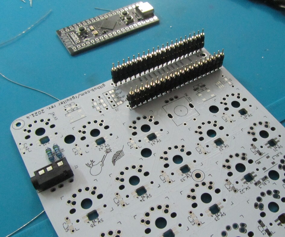
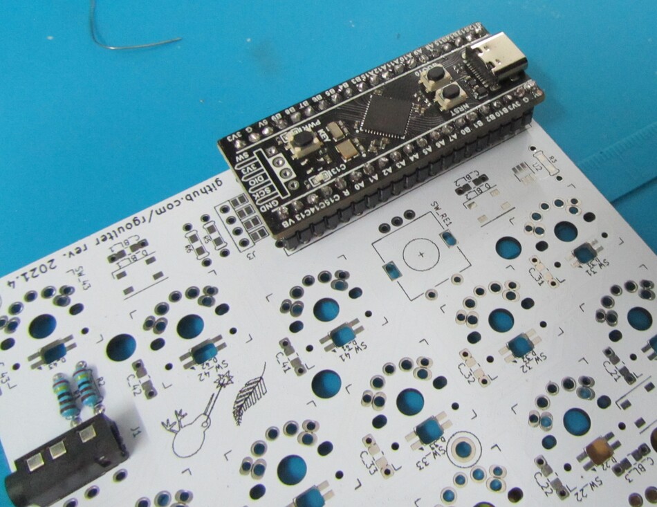
- Solder female headers in appropriate pads at U1, and solder the microcontroller to the male header pins.
- Solder in the switches.
For each half:
-
Insert the through-hole resistors.
Insert resistors into the through-hole pads at R1, R2.
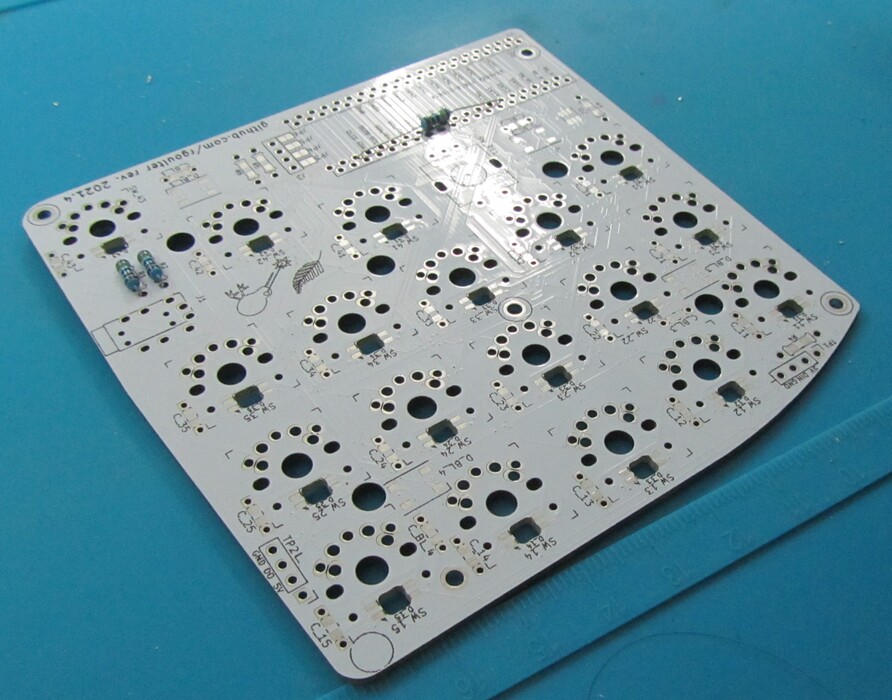
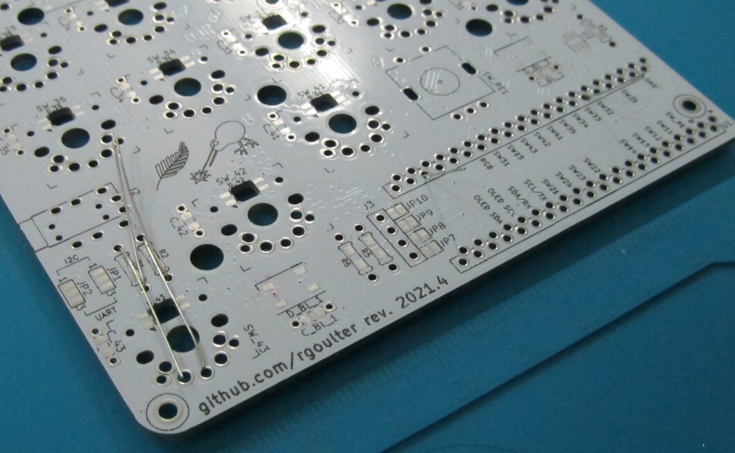
To work around qmk/qmk_firmware#7855, an external pullup resistor is needed from A9 to 5V or 3V3. Compare the location of these pins on the PCB, with where the resistor is placed in the image. (If using DIP40 socket for the microcontroller, etiher take care to position the resistor so it doesn't obstruct where the DIP socket goes, or cut the DIP socket).
i.e. on the Left Hand Side, you'll want to pull up:
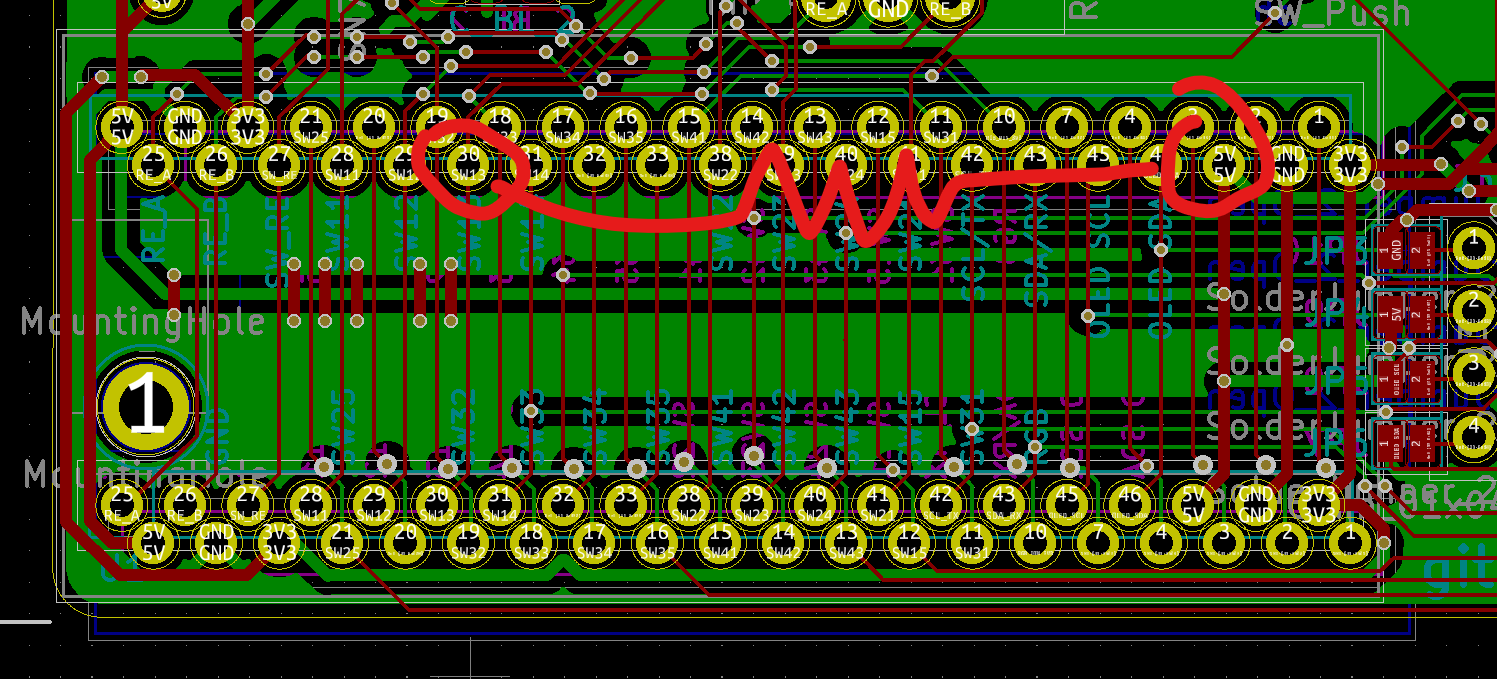
and the Right Hand Side:
-
Solder the resistors.
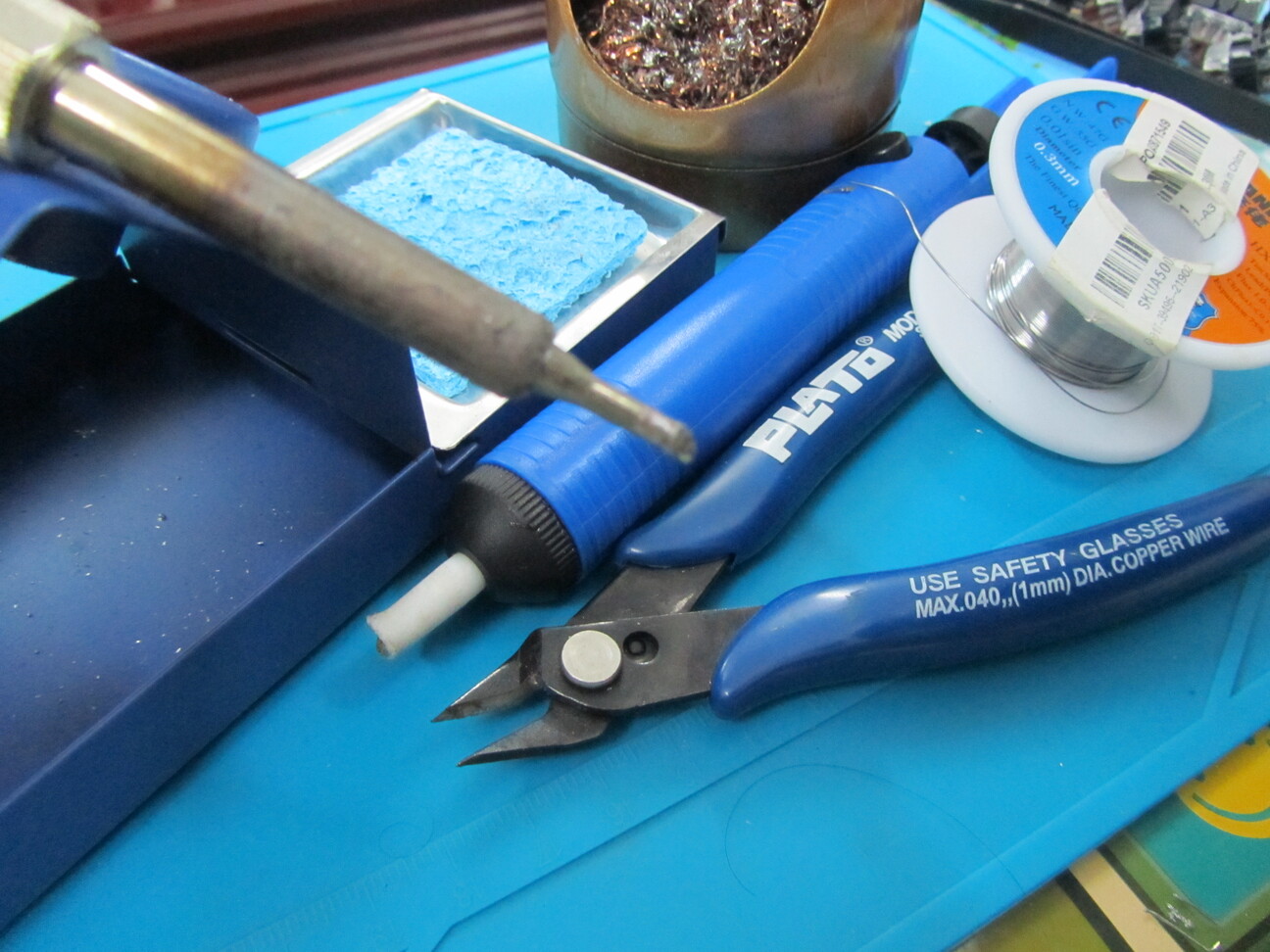
If you've never soldered before, best to search for "how to solder through hole components" to get an idea of what it should look like.
Use the flush cutters to cut the legs of the soldered resistors. Take care to protect your eyes when using the flush cutters (e.g. by wearing safety glasses).
-
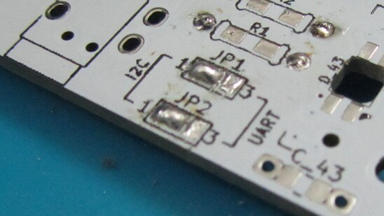
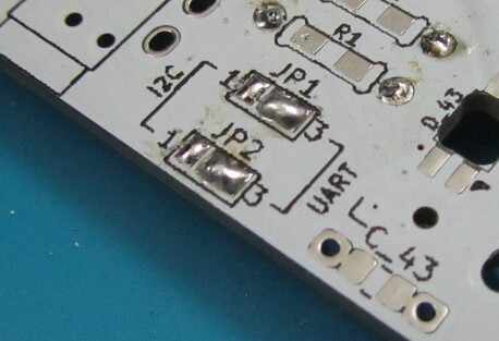
For the Right-Hand Side PCB only: On the top-side of the PCB, use solder to bridge JP1 and JP2 to either 1 or 3.
Currently, the QMK firmware only supports JP1 and JP2 jumped to 1, the Keyberon firmware only supports JP1 and JP2 jumped to 3.
i.e. for QMK, it should look like:
i.e. for Keyberon, it should look like:
-
Solder the TRRS jack.
Place the TRRS jack on the top-side of the PCB.
Solder one pad first, check that the jack sits flush with the PCB. It's easier to heat the soldering and adjust the positioning of the TRRS jack with only one pad soldered.
Solder the remaining pads once once it's in place.
-
Solder in the female headers and/or socket.
Cut each of the 1x40 headers in half so that they can be used to socket the PCB and microcontroller.
I suggest first soldering in the pins at the end, then insert the round-pin male headers. Ensure that the development board sits evenly.
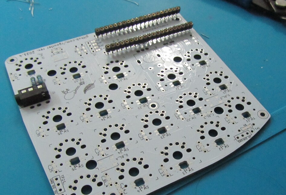
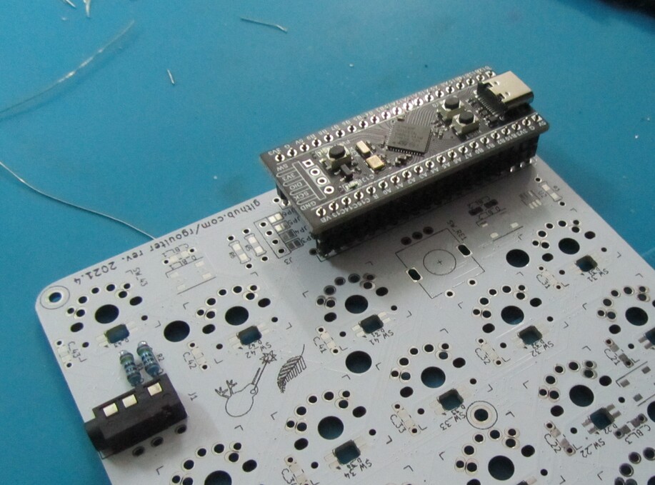
Then solder the rest of the female header pins.
The soldering can be 'tidied' a bit by cutting the soldered pins flush with the board, and then adding a bit more solder so the soldering is 'round'. c.f. https://makerprojectlab.com/how-to-make-beautiful-solder-joints/
-
Solder the development board to the round male header pins.
-
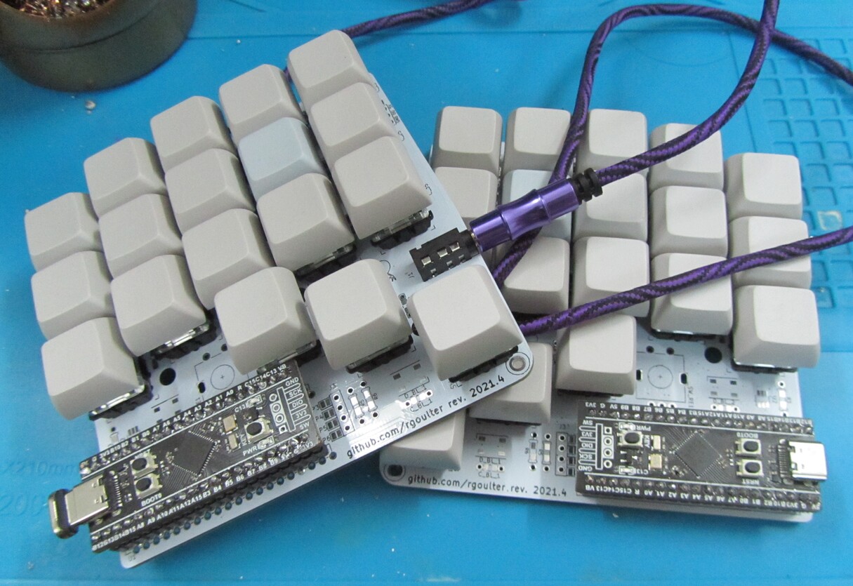
Insert the MX switches. Ensure each sits flush with the PCB.
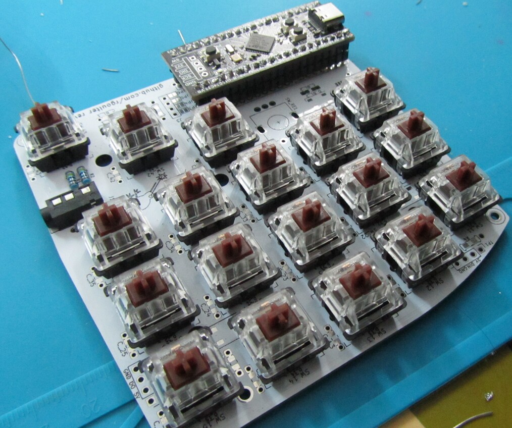
Solder both legs of each switch. Take care to not create shorts between the adjacent pads.
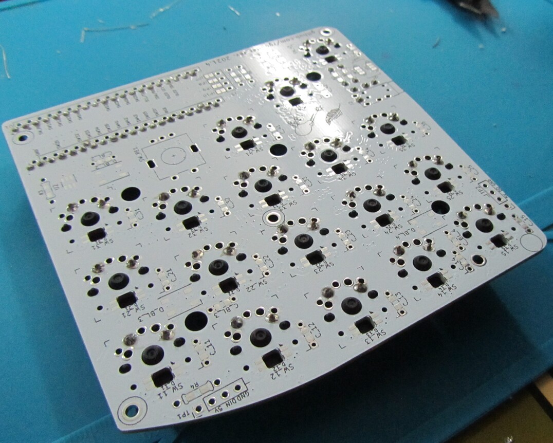
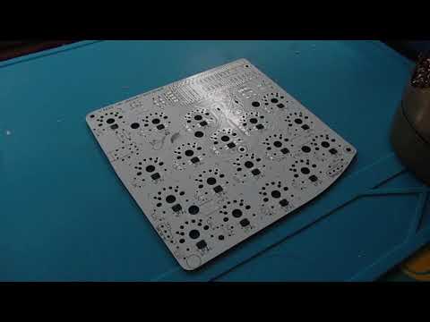
All the soldering is finished.
-
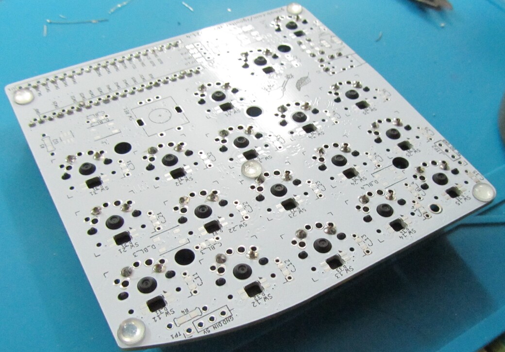
Complete the assembly by placing the keycaps.
Also place bumpons on the underside of the PCB.
See the repository's readme for instructions on building and flashing the firmware.
The keyboard firmware using keyberon uses UART to support the split keyboard functionality. (i.e. LHS's 'TX' should be connected to RHS's 'RX'). The QMK firmware relies on QMK's split-common serial transport. (i.e. LHS's 'SCL' should be connected to RHS's 'SCL').
Compare the schematic:
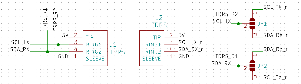
with JP1 and JP2 bridged to 1:
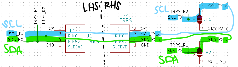
with JP1 and JP2 bridged to 3: