these are the instructions to build the INA3221 based prototype.
We will start with a 5x7 CM prototyping board.
The first thing will be to drill the fixation holes to 3,2mm. The corners will break, but that does not matter. I have carved edges to fit into corners of my box, done a bit too much damage.

The 0.1 Ohm SMD shunt resistors will enable measurement up to 1.6Amps only, which is okay for a 20W panel (version without SZBK power buck).
For bigger panels you need to replace the SMD shunt resistors with 0.01 Ohm or even 0.005 Ohm models. Do not worry, replacing these kind of shunts is not rocket science.
Just put a good quantity of solder tin on the terminals and heat in short sequence both sides, then quickly shift away the SMD resistor with the tip of your iron.
You can do that! I could also, and I am an old man, not very far from getting Parkinson.
Then position the new resistor inplace and solder first one side, while you hold the item, then solder the other side with enough tin, and come back to the first side with fresh tin.
Then we will solder the screw terminals. I had two- and three- blocks available, which will allow me to place the ground terminals beneath the respective positive terminals, which is a somewhat more logical disposition. On the top side of the INA module, I am usually soldering a strong wire bridge between the 2 GND holes, useful to clamp the GND of a multimeter.
If you only have 2-blocks, you can solder them directly onto the GND holes.
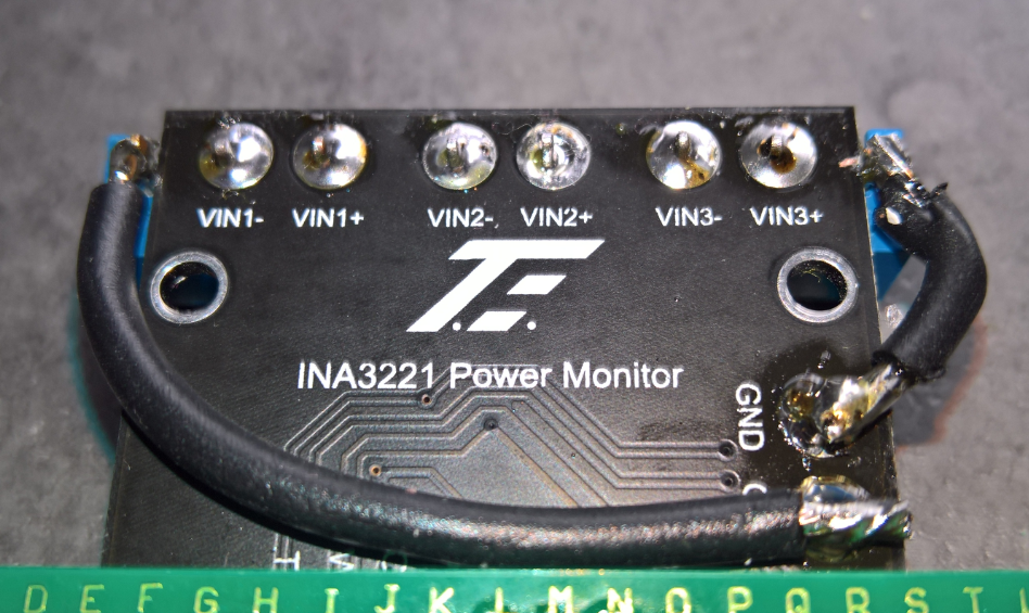 Then solder the 8 pins on the INA module and then on the top line of the prototyping board between the rows H to Q.
On the back, cover the soldering bridges labeled “ADJ” to “1,8V” with some scotch tape. Then, glue a heat sink. I am using Pattex Fix Nail power from the construction market.
Solder a five pin male header to the 4 pads of the module leaving one pin right of the pad VO+ free.
Solder a thin yellow wire between that free pin and the upper right corner of the trimming pot. It is tiny, you need a fine solder tip!
Bring first a pinhead of tin to the edge of the potentiometer, tin the ned of the wire and then solder the wire inplace.

The "Fine Red" buck converter fits ideally under the Wemos D1 and delivers a 5V USB plug, situated just under the USB connector of the WEMOS-D1:

To solder this module on the prototyping board, we will use a direct solder connection between the two boards.
First of all you need to prepare the module, which back should be as flat as possible.
Cut the pads from the USB connector with a cutting plyer as flat as possible.
Then put a generous quantity of solder tin on the outside USB connections:

Solder a provisional wire bridge on the input ports leaving 1cm wire in excess at the other side.

Place the converter on the prototyping board in such a way is that these wires fit into the holes J-09 and O-09, solder these two holes.

Then the two outside USB connections should be exactly under the holes K-03 and N-03. Press firmly the two boards together prototyping board atop and introduce a piece of wire in the holes K-03 and N-03 filling generously with tin so the molten tin will folow the wires and contact through the red board.
The two boards should now be firmly connected together.
Then cut the wire bridge at the other side and test your connections:
If you suply 12V, (+ to O-09 and - to J-09), you should get 5V (+ at N-03 and - at K-03).
Solder the female short pin connectors between H02 to H09 and between Q-02 and Q-09.
Solder the female long pin connectors through the Wemos D1. you can then plug the WemosD1 onto the board and optionally the OLED display on top:

Who has the skills and wants to make a PCB for the project? I just never made it and don't want to learn that now...
- Place the components according to the picture bending the pins to adjacent destinations, so you do not need extra wires. (shown grey in the drawing)
- Solder the GND trace according to the picture. (shown fat black in the drawing)
- Solder the red +5V Vcc line according to picture (the dotted red line would have been for a HW813 module)
- Solder the orange +3.3V Vdd line according to picture (the dotted orange line passes on the other side of the board)
- Solder the 2 violet Relay lines according to picture
- Solder the white A0 line according to picture (shown double grey between Q08 and U07)
- Solder the 3 blue Enable lines according to picture
- Solder the brown and green I2C lines according to picture
- Solder the 2 yellow injection lines according to picture
The curved thick power lines orange for panel, red for Battery and violet for Convenience are intended to be soldered lose between the prototype board and the attached INA3221.

The finished board:

(the green I2C line is grey in my build)
The front side:

Tomorrow I will build it into the box...
Enjoy!
...to be continued.