Project of Addison Elliott and Dan Ashbaugh to create IC layout of 32-bit custom CPU used in teaching digital design at SIUE.
Note: This guide contains information based on Addison and Dan's experience with the Cadence tools during the 1 month period spent on the project. As a result, this guide may contain mistakes or incorrect information and pull requests are welcome to fix any issues.
- SIUE CPU IC (SCIC)
- Table of Contents
- Overview - Block Diagram
- Setup
- Workflow
- Simulation
- Synthesis - Reports & Menus
- Place & Route
- Final Steps
- Results
- Workflow Commands List
- Future Work
- Simulating with Icarus Verilog
In the introduction class to digital design at SIUE, there is a simple CPU written in Verilog that is used for demonstration purposes. The design is discussed and simulated but never synthesized, whether it be on an FPGA or ASIC. In this project, we took the CPU from this class and created an ASIC design using the Cadence toolset making some minor changes and additions to the CPU itself.
Note: The original CPU from the digital design class can be found in the old_files folder of this repository.
Specifications:
- 1x 32-bit accumulator (AC)
- 32-bit instructions (1 word)
- Bidirectional I/O port (input = switches, output = LEDs)
- RAM
- ROM
- Non-pipelined implementation. Clocks per instruction (CPI) = 2
- 32-bit adder
- 4-bit opcode, 9 instructions, 16-bit address space
- Behavioral implementation
Instruction format for the CPU is as follows:
    31----28------------16-15----------------0
     Opcode    Unused            Operand
The updated CPU that we worked on contains the following instructions (bolded instructions are new):
| Instruction | Opcode | RTL |
|---|---|---|
| Add | 1 | AC <= AC + mem(IR[15:0]) |
| Shift Left | 2 | AC <= AC << mem(IR[15:0]) |
| Shift Right | 3 | AC <= AC >> mem(IR[15:0]) |
| Load immed. | 4 | AC <= IR[15:0] |
| Load | 5 | AC <= mem(IR[15:0]) |
| Or | 6 | AC <= AC |
| Store | 7 | mem(IR[15:0]) <= AC |
| Branch | 8 | PC <= IR[15: 0] |
| And | 9 | AC <= AC & mem(IR[15:0]) |
Address range for the memory controller is as follows:
| Name | Range | Size (words) | Binary Range |
|---|---|---|---|
| ROM | 0000-001F | 32 | 0000 0000 0000 0000 -> 0000 0000 0001 1111 |
| RAM | 0020-003F | 32 | 0000 0000 0010 0000 -> 0000 0000 0011 1111 |
| I/O | 0040-005F | 32 | 0000 0000 0100 0000 -> 0000 0000 0101 1111 |
Test ROM Program to fully test all the instructions:


Note: This was run using Dr. Engel's special workflow with custom TCL scripts. You must do this using the lab machines with their custom scripts in order for this tutorial to work.
Begin by logging into a VLSI lab machine in EB3009 and then open a terminal. Run the following commands to get your terminal setup with Dr. Engel's custom scripts. These commands only need to be run once each time you open a terminal to setup your environment correctly.
cds_ams
cd $PHOME
setup_edi
Navigate into verilog.src and clone the project repository with the following commands. Note: If you are wanting to push changes back to the repository eventually (requires write access), then you must use the following URL rather than the one given below https://<GITHUB_USERNAME>@github.com/addisonElliott/SCIC.git.
cd verilog.src
git clone https://github.com/addisonElliott/SCIC.git
The directory verilog.src contains all Verilog projects that are going to be simulated or synthesized using Cadence. This is a custom directory structure setup by Dr. Engel to adhere to his specific workflow. The purpose is to standardize where projects are located for ease of use. Cloning the repository only needs to be done once because afterwards it will be stored on your machine. But, if you want to pull new changes from the repository, you can do so with the command git pull origin master. You must be inside the directory to run the git command (or any git commands for that matter).
Next, one more once-per-machine step must be done. There is a TCL and SDC file that is expected to be in a different directory to adhere to Dr. Engel's workflow. Since we wanted to make these files tracked by our GitHub repository, we place these files in the repository and create symbolic links (i.e. symlinks) to these locations. Run the following two commands to create symlinks for the TCL and SDC file in the appropriate directory.
ln -s $PHOME/verilog.src/SCIC/env.SCIC.tcl $PHOME/env_files/
ln -s $PHOME/verilog.src/SCIC/SCIC.sdc $PHOME/verilog.src/sdc/
If you want to verify that the symlinks were made, take a look at the figure below where I used the ll (alias to ls -l) command to achieve this. You can see that the output shows a symlink pointing to the repository location.

Once the repository is cloned and setup, one remaining command must be called. This command must be called each time a terminal is opened to set the current base project. sb is a script written by Dr. Engel and is short for set base to set the base project. The argument to this script is the name of any project contained in the verilog.src folder. To see the current project, you can type b for the base project. The workflow commands used below use the current "base project" to perform their respective actions on.
sb SCICThe general workflow for synthesizing a Verilog project to an IC can be seen below. Preceding the RTL simulation is developing the Verilog module, general setup of the project and creating the SDC & environment TCL file. While developing your project, it is extremely common to encounter an error in one of the steps, in which case you will correct the error and restart the workflow.

The first step of any design is to simulate the Verilog code using a testbench to ensure that it is performing the way it is designed. There are three cases throughout the workflow that a simulation is performed.
- RTL Simulation (rtl)
- Ideal simulation with no delays included. Used to verify design functionally works
- Post-Synthesis Simulation (syn)
- Performed after synthesis and includes propagation delay for gates (no wiring delay is included)
- Post-PNR Simulation (pnr)
- Performed after place & route and includes the wiring delay as well as the propagation delay for gates
- This is the final simulation and should mimic the real-life waveforms present on the chip
The simulation in each case can be ran the same way except for one minor change. The env.SCIC.tcl file must be edited to set the simulation mode to the desired mode. Editing the file can be done using your favorite text editor (gedit, vim, nano, etc). Change the line SIM_MODE to the desired mode.

Run the following commands to simulate the design. There is no need to run the cd command if you are already at $PHOME.
cd $PHOME
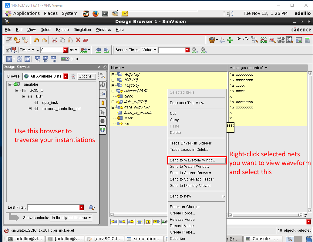
simCadence's simulator software SimVision should pop up. There will not be a detailed discussion on using SimVision, since it is fairly self explanatory. You can navigate through the Design Browser on the left to find wires that you want to add to the waveform window. You can add them by right-clicking and select "Send to Waveform Window". Once you have all the wires you want in the Waveform Window, you cans elect the "Play" icon in the toolbar to run the simulation. There is a bar at the bottom that can be dragged to change at what point of time you are viewing. See screenshots below for details on the process described.
Note: To make your life easier, you can save your current setup in the waveform window by clicking File -> Save Command Script and save the file as restore.tcl which will automatically be loaded each time a simulation is ran. This saves you the trouble of having to add the same wires to the waveform window.
See the results section for screenshots of what you should see for this step (Click here)

Before running a Post-Synthesis and Post-PNR simulation, you must type the following command to create special testbenches that include delay information. The delay information from the synthesis and place & route step are stored in a Standard Delay Format (SDF) which is loaded in the testbench using the $sdf_annotate function. Open up the generated testbenches to see the differences yourself!
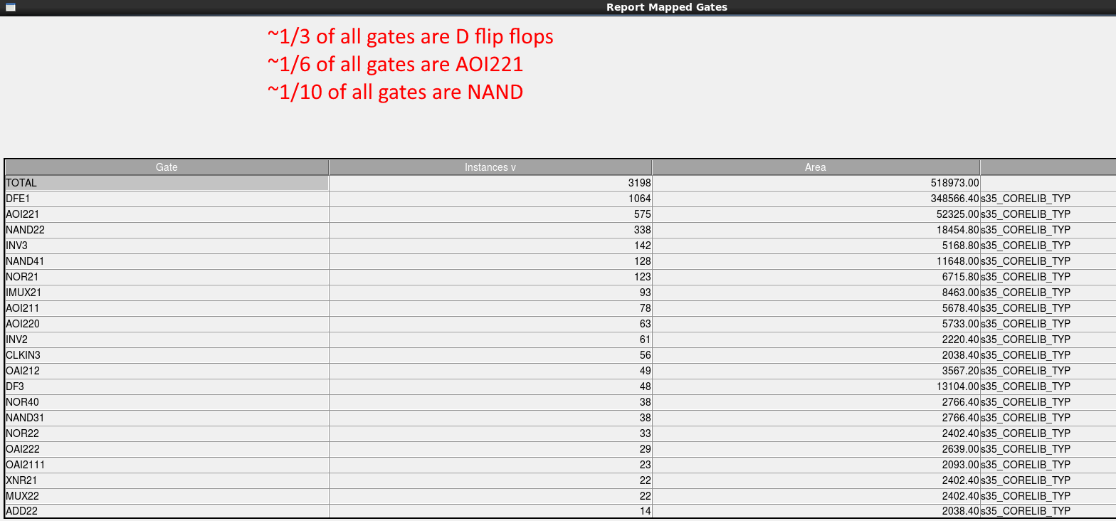
sdfAfter running a RTL simulation to verify the functionality of the project (Click here), the next step is to synthesize the design using the RTL Compiler (rc). Synthesizing the design, in this context, means to take Verilog and turn it into a purely structural design in terms of the standard cells available to the process (e.g. AOI22, NAND22, NOR22, inverter, D flip-flop). If the Verilog code is already purely structural, then the synthesize tool will not be able to optimize the design much.
Additionally, the synthesize step will also calculate the worst case timing path, total consumed area for each Verilog module instance, total consumed power for each Verilog module instance and much more. This is the point in the design where you can analyze the design and see if the area, power, timing meets your requirements.
In simple terms, the synthesize step encompasses figuring out all the gates, flip flops and components that are required and how they should be connected to achieve certain constraints. The synthesize step does not take into account wiring resistance or capacitance.
One important component for the synthesis step is the SCIC.sdc file, which is a TCL script that specifies constraints for the synthesize tool. Please see the comments of the SDC file for detailed explanation of the commands (https://github.com/addisonElliott/SCIC/blob/master/SCIC.sdc).
The synthesis tool does a lot of optimization such as removing unused registers, unused wires and any other unused logic. The tool attempts to meet all constraints in the SDC file first and it's next priority is minimizing area. An example of this that puzzled us at first was the synthesis of an adder. If the clock speed was slow enough then a ripple-carry adder would be used because it minimizes area and meets timing constraints. However, as the clock speed reaches a certain point, the ripple-carry adder becomes too slow and the synthesizer optimizes to use a carry lookahead adder.
Another frustration with the synthesis tool with optimization is that it can be difficult to probe the testbench wires because some of the wires may disappear, become high impedance or change due to the fact that the synthesis tool optimized them away. The best way I found to counteract this effect is to use the set_dont_touch command on the net in the SDC file, but even then it was a bit buggy with the results. Personally, I think the easiest solution is to ensure that the wires you want to observe are present in the testbench. Don't rely on probing internal wires because they may be missing.
Run these commands from your terminal to launch the RTL compiler:
cd $PHOME
syn
The syn command is a custom TCL script written by Dr. Engel and a former graduate student that runs the RTL compiler and runs a synthesis script within it. It will begin by parsing the SDC file and afterwards the script will pause to wait for user input. You will read the output in your terminal to ensure there were no errors, and if so type 'resume' in the terminal.
The script will finish running and then a schematic window will appear. You can double click on any of the blocks in the hierarchy to view a schematic for them. In addition, the "Report" menu provides useful options for analyzing various aspects of the design (power, area, timing, etc).
See the results section for screenshots of what you should see for this step (Click here). The synthesis should only take around 5-10minutes to complete. Don't forget to run Post-Synthesis simulation to verify the synthesis is working correctly. The simulation should show delays between signals now.

- Report
- Datapath
- Information about any datapath elements used, in our design there were none so this does not provide any useful information.
- DFT
- Design For Test
- None of these options do anything for our project
- Netlist
- Area - Area by each Verilog module split into cell area and net area summed to total area in square micrometers

- Mapped Gates - Lists each gate used, the number of instances in the design and the area these take

- Statistics - Displays area and percentages of sequential, inverter, buffer & combinational logic

- Violations - Displays any DRC violations that occurred during synthesis

- Area - Area by each Verilog module split into cell area and net area summed to total area in square micrometers
- Power
- Detailed Report - Displays dynamic and static power for each Verilog module

- RTL Power - Blank for this project, unsure what it does
- Library Domains - Blank for this project, unsure what it does
- Power Domains - Blank for this project, unsure what it does
- Instance Power Usage - Displays a pie chart of the instance power (short circuit power)

- Net Power Usage - Displays a pie chart of the net power (charge/discharge capacitances power)

- Probability Histogram - Causes RTL Compiler to crash
- Toggle Rate Histogram - Causes RTL Compiler to crash
- Detailed Report - Displays dynamic and static power for each Verilog module
- Timing
- Endpoint Histogram - Displays a histogram with the slack values for each path and number of occurrences

- Lint Report - Displays any issues with meeting timing constraints
- Worst Path - Displays slack for worst case path

- Endpoint Histogram - Displays a histogram with the slack values for each path and number of occurrences
- Datapath
- Tools
- Object Browser - Allows browsing of the synthesized logic, includes every single net, instance, flip flop and gate that is used and allows for easy traversal.

- Object Browser - Allows browsing of the synthesized logic, includes every single net, instance, flip flop and gate that is used and allows for easy traversal.
- File
- Source Script - Can be used to load an existing synthesis. For any project, the script you want to load is /opt/home/campus//cds/ece484/syn_dir/dsn/<PROJECT NAME>/<PROJECT NAME>.rc_setup.tcl

- Source Script - Can be used to load an existing synthesis. For any project, the script you want to load is /opt/home/campus//cds/ece484/syn_dir/dsn/<PROJECT NAME>/<PROJECT NAME>.rc_setup.tcl


The place & route stage is when the magic begins to happen taking a Verilog design and placing all the necessary transistors as well as connecting them up correctly. It is a complex process, consisting of many stages, to ensure that timing and other constraints specified in the SDC file are met. As a result, this part of the process may also take the longest (expect somewhere between 10minutes to an hour depending on constraints specified). Obviously, the stricter the constraints on the design, such as timing specifications, area, spacing between rows for wires, will mean that the place & route tool will take longer to complete. The place & route tool created by Cadence is Encounter (enc).
Once Dr. Engel's custom place & route script is done running, one important comment to make is that you can perform additional actions on the design in Encounter. Everything in the custom script has a GUI counterpart that can be ran. Things such as rerouting, verifying geometry & connectivity, moving wires, etc can be done after the fact.
Based on my personal experience of the software, some designs may end up with DRC violations after the process is done. The automatic router is not perfect and can leave violations after completion. Keep this in mind and be prepared to fix small issues if necessary.
There are some 'knobs' that one can tweak in the env.SCIC.tcl file for adjusting how the place & route tool will operate. These options are discussed in further detail in the comments of the file (https://github.com/addisonElliott/SCIC/blob/master/env.SCIC.tcl). Briefly, the important parameters that we tuned in this project were the router used (nano or wroute), aspect ratio, core to boundary distance, utilization (i.e. row density) factor, row spacing between transistors and pin spacing.
One frustration that we ran into during this project is that after completion, there would be on the order of hundreds of DRC violations. After much experimentation and review of our Verilog code, we came to the conclusion that has something to do with the router used. The default router used is wroute which is Cadence's old tool and was superseded by nano. According to Cadence's documentation, nano is recommended for sub-180nm processes or larger projects with more than 300K instances. Dr. Engel also informed us that the nano router was recommended by the AMS engineers over the wroute router (even though our process is 0.35um). But, Dr. Engel and his students empirically found that wroute yielded better results than nano. With all this in mind, the important thing to take away is to try multiple routers and try running route multiple times. Using the nano router in this project solved all DRC violations in Encounter.
Now with that introduction, let's begin running the place & route tool.
cd $PHOME
pnr
Similar to the syn command, the pnr script was written by Dr. Engel and his graduate students. The encounter log window keeps you informed as to exactly what the tool is doing but you will also see a bunch of text spewing across your terminal. Multiple times throughout the script, the script will be suspended and will wait for user input to continue. If you follow the instructions on the log window, you will be fine!
The script will start by creating and setting up a floorplan before stopping to ask for user input. At this point, your job is to review the floorplan and make sure you're happy with it. Open the Encounter window (should pop up on its own) and zoom in to the rows. You want to verify that you have enough space between the rows of transistors (we made ours 30um). Additionally, zoom in at the top of the design and you should see the pins placed. You want to verify you have enough spacing between the pins to allow for routing and also enough spacing from where the pins are to where the design starts, i.e. core to boundary distance. Type 'resume' when you're happy with everything.


The next part of the script will take the longest because it is actually placing the transistors and routing them. The next time the script stops is after everything is completed to allow you to check for DRC violations. Throughout most of this step, there should be text spewing out on the terminal window describing what is going on. At one stage, it will attempt to meet timing constraints and will iteratively print out slack (remember, negative slack is bad!) and will slowly attempt to make the slack positive (0.1ns). If your timing constraints are too strict, then this will take awhile and will eventually give up and stick with the negative slack. If you're not paying attention to the screen at this moment, there is no further indication that timing was not met, so keep that in mind. For this project, we have a period of 10ns (100MHz) and this process stops around -2.5ns slack. This means that the maximum clock speed we can have is 80MHz (12.5ns period).
Note: During the synthesis step, the RTL compiler attempts to achieve minimal positive slack and then minimize area. This is not ideal because the place & route tool will have a harder time to keep the positive slack. As a result, one workaround is to use the set_clock_uncertainty SDC command to add a "margin" to the slack in the synthesis tool. In theory, this should make it easier for the place & route tool. However, during our project, this did not seem to help reduce the slack much. One possible reason is that the SDC file is also used in the place & route tool and the set_clock_uncertainty is copied again. Separate SDC files for the synthesis and place & route step may be one solution but further testing is warranted.
After the script has stopped again, you will want to look at the terminal for geometry or connectivity violations (i.e. DRC violations). If there are issues here, there will likely be LVS or DRC errors later on. Any DRC violations will also be shown as white X's on the design in Encounter. You can zoom in and click on the white X to see what the violation is. In addition, there is a Violation Browser in Tools->Violation Browser that is helpful for viewing violations.


DRC violations will occur in this project and the solution is to run again with a different router. Type the following commands into the terminal (it accepts TCL commands when suspended).
amsRoute nano
verifyGeometry
verifyConnectivity -type all
Once there is no DRC violations, type resume once again to finish the design by placing power pins. At this point, you can close Encounter and move to the next step.
See the results section for screenshots of what you should see for this step (Click here). Don't forget to run Post-Synthesis simulation to verify the synthesis is working correctly. The simulation should show delays between signals now.
This completes the use of the Encounter Digital Implementation (EDI) tools. The final step is to convert the layout & schematic to Cadence Virtuoso. This can be done with two simple commands, given below. Note: You must call edi2ic first because it wipes the ediLib section while edi2sch does not.
edi2ic
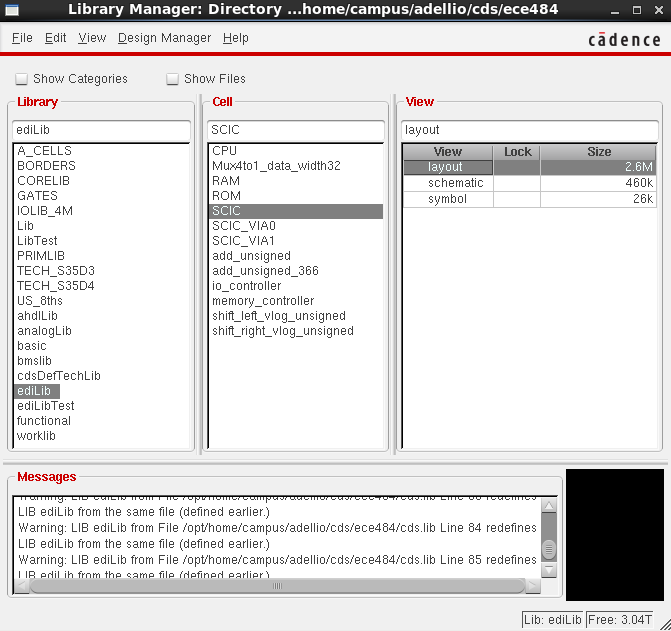
edi2schNow the layout & schematic can be opened in Virtuoso like any design. Start Virtuoso (using icd_ams command) and select ediLib -> SCIC and double-click on the layout. Run LVS and DRC checks to ensure there are no issues.
✨ ✨ ✨ ✨ ✨ ✨ You are finished with your design! ✨ ✨ ✨ ✨ ✨ ✨
The remainder of this document is additional information and results from this project.
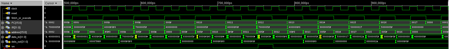
Keep in mind that the only purpose of the RTL simulation is to verify the functionality of your design. From the images below, it is clear that the CPU is working as intended. The fetch_or_execute register is switching between fetching and executing, the PC is incrementing every 2nd clock cycle and the IR is loaded with each program instruction correctly. The AC register is displaying the correct results for each of the operations.


The important peice to note here is that the results are the same from the RTL simulation. The only exception to this is that there is no AC wire because that was optimized out. The value on data_out is the same as the AC register however. In addition, you can see a slight delay and ringing between when the clock edge occurs and when the other wires change.

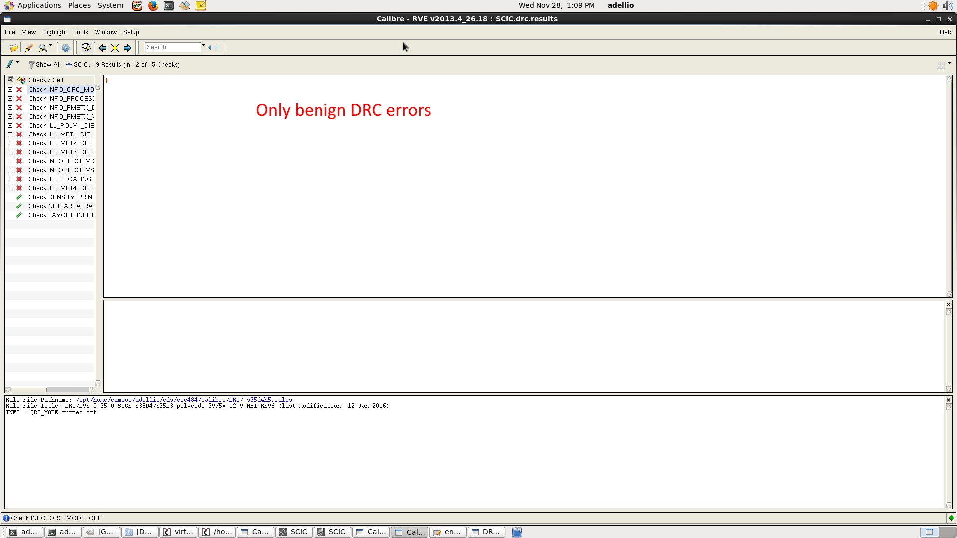
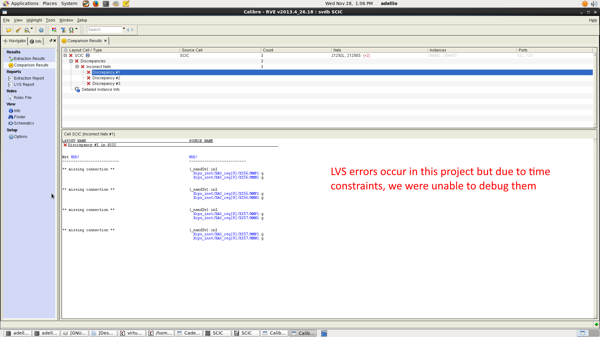
Zero DRC violations when running nano router after wroute. See the steps above for more information. Design looks good and seems well routed. However, minimum slack was -2.5ns which means we can only run this at about 80MHz. In addition, there are 3 minor LVS errors that need to be resolved. DRC errors are just the benign typical ones, thus DRC was successful.


Looks same as post-synthesis simulation.
- Area: 2100um x 2100um
- Maximum clock speed: 80MHz
# Setup terminal
cds_ams
cd $PHOME
setup_edi
sb SCIC

# RTL Simulation
# -----------------------------------------------------------------------------------------------------------------
# ACTION: Edit env.SCIC.tcl to set SIM_MODE to rtl
sim

# Synthesis
# -----------------------------------------------------------------------------------------------------------------
syn
# ACTION: Follow command prompt and review timing, power & other constraints in GUI that appears once synthesis is
# done

# Only needs to be done once
sdf

# Post-Synthesis Simulation
# -----------------------------------------------------------------------------------------------------------------
# ACTION: Edit env.SCIC.tcl to set SIM_MODE to syn
sim

# Place & Route
# -----------------------------------------------------------------------------------------------------------------
pnr
# ACTION: Follow command prompt and review layout after finished
# ACTION: Quit encounter once layout is complete

# Post-PNR Simulation
# -----------------------------------------------------------------------------------------------------------------
# ACTION: Edit env.SCIC.tcl to set SIM_MODE to pnr
sim

# Final Steps
# -----------------------------------------------------------------------------------------------------------------
edi2ic
edi2sch

icd_ams
# ACTION: Go to ediLib -> SCIC, double-click layout
# ACTION: Run LVS & DRC on layout to check for errorsBelow is a list of issues we encountered but did not have enough time to investigate.
- Unable to view AC wire in simulation after synthesis
- Best solution is to ensure that any wires you want to view is included in testbench and is present at the top-level module
- Create RAM generator to allow for full 2kB of RAM, only using 64 words of D flip flops, very slow
- Optimize design to allow for full 100MHz operation
- Fix LVS errors using nano router
- Fix DRC errors when using wroute router, figure out why this occurs
Performing a simulation with Icarus Verilog is great because it is an easy-to-install tool that provides cross-platform support. This is good to use when debugging and developing your Verilog project without access to the Cadence toolset.
Note: If this is your first time installing Icarus Verilog, then you will need to make sure that the binary path is in your PATH variable. This will allow you to run the commands iverilog, vvp and gtkwave in your repository path. During installation, you will want to check the option to install gtkwave as well. Icarus Verilog must not be installed in a path with spaces or else the commands will fail. The following two paths must be added to your PATH variable:
- <IVERILOG PATH>/bin (e.g. C:/iverilog/bin)
- <IVERILOG PATH>/gtkwave/bin (e.g. C:/iverilog/gtkwave/bin)
Open a command prompt (cmd.exe for Windows, Terminal on Linux), navigate to this repository and run the following commands:
iverilog -o out.o CPU.v memory_controller.v Mux4to1.v RAM.v ROM.v SCIC.v io_controller.v SCIC_tb.v
vvp out.o
gtkwave SCIC.vcd