More compat jumpers for Teensy++ 2.0 #30
Conversation
6449829
to
ecee7ad
Compare
|
Thanks for your pull request!
Cut traces can easily be undone by soldering a jumper wire (for example) to both ends of the trace. My concern with changes that add elements to the board design is complexity: in general, I strive for minimalism in this project, to keep it accessible to people. If you still think it’s worth adding the solder jumpers, here is a bit more detailed feedback on the changes:
So, as far as I can tell, the new jumpers have the opposite semantics (bridged) compared to the old ones (open). In a way, that makes them an undo mechanism for the existing jumpers. I think it might be more descriptive to make the silk screen say e.g. So this explains why you add the jumpers, but why do the new ones use a different footprint? I think it would be more consistent to stick with the current footprint, no?
This is the first time I see cadlab.io, thanks :) In their schematic view, your jumpers don’t render. Not sure if that point will be moot with a footprint change, though.
Yes, please break these changes out separately into one Pull Request each, ideally with a rebased history and minimal changes to the schematic, to keep the history useful and accessible to people. |
That is certainly an option for cut traces, but my understanding is that in the current design, there is no single trace I can cut to make the board compatible with a Teensy++ 2.0, because the connection that needs to be broken is not a trace. The connections that need to be disconnected are between the pads 15,16,7 and the pins in the socket - so the only way to do that is removing the pins from the socket, which then makes it impossible to replace it with a newer Teensy. I could cut the traces on either side of the pad and then add wires from the existing jumper pads to the correct pins, and then later re-join the cut traces as you mentioned, but that is a lot more mess than soldering jumpers back together!
I appreciate the minimalism here! I think the addition here it is small - it's not an extra component, and the setup for the recommended Teensy 3.6 path doesn't change at all - but it does add complexity to the layout.
Correct, these are default-closed and thus opposite the others, but they aren't exactly an undo, I don't think - if I wanted to undo the existing jumpers, I would just remove the solder from them :) The first set of jumpers connects different pins to support the Teensy++, but that's only half of what's required - as stated above, you have to also disconnect the old pins so they don't interfere. That's what these new jumpers do - allow you to disconnect the old pins with jumpers, instead of removing header pins. So with this setup, for a Teensy 3.6, you would disconnect JP1/2/3, and connect JP4/5/6. This is how the design is to start, so Teensy 3.6 users don't have to do anything. For Teensy++, you need to connect JP1/2/3 and disconnect JP4/5/6, so you'd solder 1/2/3 and cut 4/5/6. And yeah, if this seems a change worth making I will certainly update the documentation accordingly!
I would have stuck with the triangles if I could, I like them! But there doesn't seem to be a default-closed version of the triangle jumpers, which makes sense since it would be harder to cut the traces at an angle like that. I could replace the triangle jumpers with the open version of the rounded ones I used for consistency instead, if that seems better. Oh, while we're talking jumpers, there is also a default-closed jumper with one wider trace instead of the two narrower ones - I just picked one, if you prefer one trace to cut per jumper it's easy to swap out the footprint!
Yeah, I found it a while back - I use it specifically for the visual diffs so I haven't used it for much else, but that's a very handy feature! It does look like they don't quite render the jumpers correctly. |
|
Thanks for the additional explanation, this change now makes sense to me. Can you move the new trace for signal Also please update the solder instructions, rebase your changes on the current master branch contents, and clean the git commit history. Thanks! |
|
Great, will do! What do you think about the existing jumpers? Should I replace the triangles with circles to match, or leave the triangles in place because they look nicer? |
|
Oh, and also that's where I originally had the
|

765c8d3
to
641db4a
Compare
|
Okay, on investigation moving I've also taken a run at updating the instructions and rebased on current master. I'll clean up the history once I'm sure it's all settled. Should I also take new screenshots once the board is settled and update the readme with them, or do you want to do that? |
I think replacing them for consistency is better.
Thanks for looking into it! Can you add a screenshot please?
I can take care of updating the artifacts when tagging a new revision. |
3ad47ff
to
f62343a
Compare
|
Okay, great - I've updated the jumpers to be consistent and squashed down to two commits, happy to combine it all down to one if you prefer. And here's a screenshot of the |

README.md
Outdated
| @@ -219,8 +219,8 @@ the same time :-). I want to add an edited and higher-quality video, too. | |||
|
|
|||
| 1. Place your Teensy 3.x or 4.x on top of the pin header and solder all its pins. | |||
|
|
|||
| * If you’re using a Teensy++ 2.0, you must not connect some pins! [See the | |||
| instructions below](#soldering-instructions-for-the-teensy-20). | |||
| * If you’re using a Teensy++ 2.0, you may want to remove some pins before | |||
There was a problem hiding this comment.
Here and below, I think we can make this language stronger: there’s no need to keep the plier method around. Let’s just recommend people close JP1-JP3 and open JP4-JP6 for Teensy 2.0 support.
One commit for the board change and one commit for the README change is great, thanks :) |
|
@cincodenada Are you interested to finalize this contribution? If you rebase the commits there will be conflicts to resolve in the pcb and schematics files. Do you have experience resolving such conflicts? Would it be easier to simply redo the changes on top of latest master? How much time do you think this would take? Thanks! |
|
Oh hey, thanks for the ping, this fell off my radar. I think I stalled here because after putting this together myself, with the headers I initially used, a removable Teensy didn't quite have enough headroom, and the case wouldn't close all the way. But I have since found that using shorter, socket-style headers solves that problem nicely, and then never circled back to update this. So anyway - I have actually done a lot of messing about with rebasing schematics files and the like, so I'll give it a run and see how things fall out - how painful it will be depends on what has changed in the meantime! |
|
I made a pull request to update the project format to KiCad 6.0. This would make impossible to resolve the merge conflicts with this branch. How do these shorter socket-style headers look like, can you post a picture please? If that's an alternative then we might not need this change after all because one can easily replace or add a missing header? |
|
For my noob curiosity, how much time would it take to re-do the changes, and how would one go about it? |
|
Thanks for the bump here, I forgot about this last weekend. The changes are fairly simple conceptually, but involve some lengthy routing, which makes the boardfile possibly tricky - if you can just re-run the traces as they are in this PR, it's pretty straightforward to just re-do them, perhaps even easier than trying to merge. I wasn't terribly clear above - the shorter headers aren't an alternative to these jumpers, rather the shorter headers make this PR more useful - with tall headers, socketed Teensy's wont fit in the case at all, so it makes less sense to account for switching out Teeny's (which is what this does). Anyway, I've got things just about merged now - I merged in the version just before the v6 upgrade, then saved that in KiCad 6, and am finishing merging the result. Which was in retrospect probably not super necessary, but I'm most of the way there now, ha. |
|
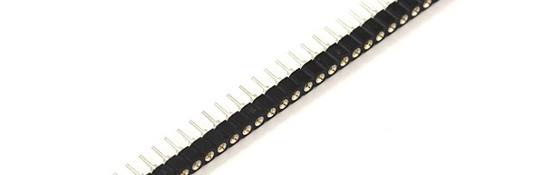
From what I read, I see these shorter header pins are called "swiss pins" on Adafruit, "[swiss] machine pins" on Sparkfun and "round pins" on AliExpress. They are not always compatible with regular pins due to the different leg length and profile. The round pins are 0.5mm diameter vs the square pins 0.6mm side, 0.84mm diagonal. The physical connection made by the round pins is considered superior to the normal header pins. Fun fact: The male round pins have one leg with diameter 0.5mm and the opposite with diameter 0.6mm. |
|
Oh, I already ordered a bunch of different low-profile pins and tested them, including some of the "swiss pins" - they are indeed one style, and have their advantages, but unfortunately they are, as you noted, round and not compatible with the usual jumpers found on a Teensy, but you could probably outfit the Teensy and KinT with them if you wanted. Fortunately, there are also regular square headers available in a low-profile style: https://www.digikey.com/en/products/detail/samtec-inc/SLW-124-01-T-S/1104812 This is what I have on my KinT (ignore the weird mismatched sides, I somehow ordered the wrong length): These allow using a Teensy with traditional socket headers. I also used shorter pin headers for my setup, but I don't remember if that was strictly necessary or not. |


5a699ca
to
7bd283c
Compare
|
Okay, I got everything merged in and updated, and then squashed things down to two commits. I also did some further updates to the readme, to remove references to removing pins, and also add a section about using headers, based on my experimenting. I realize it's perhaps a little silly adding this now that the Teensy 2.0 is officially discontinued, but I think if we're gonna support it at all, the jumpers are a notable enough improvement to doing so that it's still worthwhile anyway. In case anyone is curious about the details of the merging, I put the original merged branch up at more-compat-jumpers-merge on my fork. |
7bd283c
to
dcc11ab
Compare
a71211e
to
6451b69
Compare
|
Is this ready for review? |
|
ping |
6451b69
to
299f344
Compare
|
Thanks for the pings! I had time to sit down today and double-check things, and yes, this should be good to review, it's all upgraded to KiCad v6 and I've added details about the headers to the README. I just rebased it against the latest main as well. |
299f344
to
2895a86
Compare
|
I pushed an update that fixed the octopart URLs. I also looked into why this PR net adds ~25k lines, nearly doubling the size of the boardfile, because there's no reason it should. Upon investigation it is a result of the zone fill polygons being much more detailed and containing about twice as many points as the old zone fills for some reason. It seems to be a side effect of a change in how KiCad generates the fill polygons, in that it no longer includes the border line or some such. I played around with various settings for a bit, but didn't find any magic bullet - if I enable "Mimic Legacy Behavior" under Board Setup->Design Rules->Constraints it helps a little, reducing the change to net 15k, but that's still a lot. If I regenerate the board fills on the |
|
If I understand correctly it seems to be due to the rounded corners: |
|
Yeah, that thread is where I learned about the border line change - but I don't think the rest of it applies here, as it's about zones with filleted or chamfered corners, and this design doesn't have either of those. I did try those options (we're already using smoothed polygons, and I upped the maximum deviation) but they also didn't appreciably reduce the size. I did some further research and comparison, and it looks like something about the algorithm for generating curves/circles changed and KiCad is basically generating twice as many points as necessary for circles. I'm actually running a bisect on the KiCad codebase today to see if I can dig in further, since as of now this seems to be a larger issue. |
|
If you click the "Update PCB with changes made to the schematic" in the PCB editor, the JP1-3 jumpers are turned to the previous rectangle-looking shape. I think the schematic has to be updated to specify the rounded corners version. Also three Also some other mysterious changes take place. What are these? Using KiCad 6.0.2 |
c6e42b5
to
c2c63c9
Compare
|
Oh goodness, I thought surely I had regenerated the board but I might not have had all the right boxes checked. I've fixed up the footprints, and regenned the board, which also seems to have resulted in a more efficient zone fill outline, and reduced the increase above. I don't think I tweaked any settings, altho I may have upgraded from KiCad 6.0.1 to 6.0.2, so maybe that did it. The mysterious net changes are just because for whatever reason the schematic decided that net should be named after the left end of the net (the JP4 jumper pad) instead of the right end (the U1 header pad), but all that changed is the name of that net, the routing and connections are still the same. Thanks for catching that! I've re-squashed things down, but if you want to see the changes, you can look at the changelog for this commit |
This avoids requiring folks to pull pins out of headers for Teensy++ 2.0
compatibility, instead just requiring them to cut the traces, which I
think is better and more importantly is reversible, so that if someone
builds with a Teensy++ 2.0 and then wants to replace it with a 3.6, they
can just re-close the new jumpers, desolder the old ones, and be good to
go.
With the new jumpers adding headers is possible, so that the Teensy is
removable without desoldering
99d42e7
to
5fe37b0
Compare
|
Finally had a chance to look at this through https://github.com/Gasman2014/KiCad-Diff, and it looks good! Thanks very much for this improvement. |
|
Merged with commit afac759 |
|
I ordered the latest master (afac759) on Aisler and I got a warning about a short: It basically says that J5 pin 1 is connected with Teensy pin 7, which is expected because JP4 is "bridged". Does the board or schematic have these checks and they should be updated? (It's a shame that JP4 is bridged but appears open, with paint between the pads. If you need to disconnect it you don't know how much to scratch.) |


|
Thanks for the test run! Is that the only short it warns about? I'd expect that if it complains about I'm not sure what kind of checks Aisler is running, but I assume it's just concerned that two nets with different names are connected, which of course normally would be bad, but with a pre-closed jumper I think that's usual, and in any case certainly what we want. The DRC does have these checks, but expects the nets to be separate (because it has information that Aisler does not, namely that the bridge is part of the same footprint as the pads, and thus is expected). In essense, KiCad trusts the jumper footprint when it says that the pads are separate nets but electrically connected, and Aisler doesn't have that information, so to Aisler it looks like a short. And in fact if I do assign both sides of the jumper to the same net then the DRC complains, because then the net is split in two as far as PCBNew is concerned - from a logical/schematic/net perspective (rather than a pure-copper perspective), the jumper pads are not connected, because the bridges are just rectangles drawn on the copper layer, rather than actual traces/pads (apparently KiCad 6 supports "net ties" which is a way to do this without resorting to graphic elements, but that wouldn't change anything from Aisler's end). All of that is a long way of saying I think this is normal and Aisler is doing its best, and I'm not sure what we can do here - I suppose we could name the other nets As for the solder mask, it looks like there's been some discussion about whether these footprints should have mask over the bridges or not - consensus seems mixed (both on that thread and generally in practice), but it would be easy enough to copy the footprints into the local library and add a keepout. And maybe even submit that as a PR upstream on the previous issue! |
|
Okay, I went ahead and opened #53 with a few changes based on the test - including creating maskless bridges and submitting that upstream, so let's continue the discussion over there! Thanks! |
|
I'm looking to start working on a board and was thinking about using the short sockets that this PR introduced.
|
This avoids requiring folks to pull pins out of headers for Teensy++ 2.0 compatibility, instead just requiring them to cut the traces, which I think is better and more importantly is reversible, so that if someone builds with a Teensy++ 2.0 and then wants to replace it with a 3.6, they can just re-close the new jumpers, desolder the old ones, and be good to go. Here's the visual board diff on CadLab.io: https://cadlab.io/project/24225/more-compat-jumpers/circuit/a2ljYWQva2ludC5raWNhZF9wY2I%3D/diff/b37687e3d403fc6781d031be97484b75ca7e9cb5
Here's what the 3D view looks like with the new jumper setup:

(This PR also includes my fiddling with the holes in response to #27 cause they were already there and I figured I might as well include them - I can break those out separately if desired!)