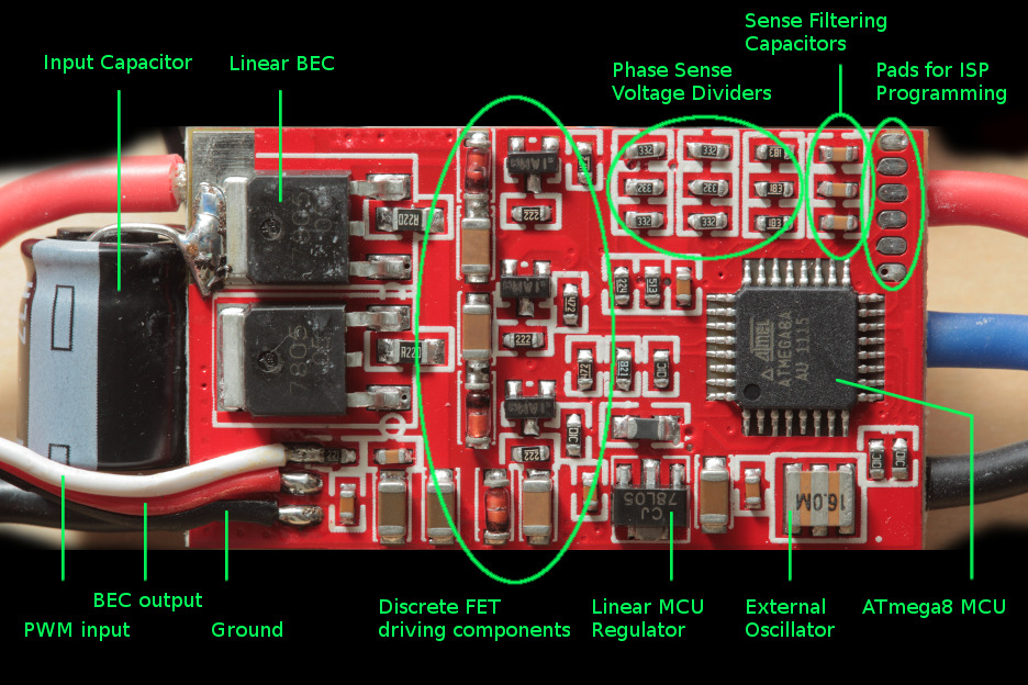
Identifying ESC pin configuration
Brushless Electronic Speed Controllers (ESCs, BL-ESCs) come in all shapes in sizes. There are three main layouts for boards most commonly found in the RC hobby market, and many ways that these layouts can be arranged and wired to the MCU. In the end, all of the different layouts accomplish nearly the same thing, with slight variations in how power is driven on each phase and the motor timing is sensed.
Identification of an ESC pin configuration is essential before attempting to reprogram it with new software. Software flashed to the MCU that does not match the pin configuration may result in immediate destruction of the ESC board, even without a motor or input attached.
- Pictures of various ESCs
- Schematics for various ESCs
- BL-ESC software projects: quax simonk wii-esc BlHeli
- Discussion threads: rcgroups helifreaks/BlHeli openpilot
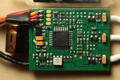
Before even considering compatible sofware, the MCU used must first be determined. Many of the common inexpensive ESCs use Atmel-based MCUs such as the very common ATmega8. These will have a chip clearly marked "ATmega8" or similar. In the last few years, some companies have switched to other MCUs such as SiLabs' F330x line, as seen on this recent Turnigy Plush 18A:
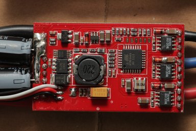
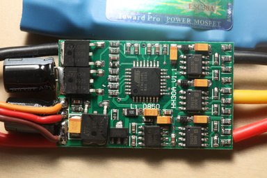
The simplest possible layout uses a combination of P-channel and N-channel MOSFETs and NPN-channel transistors for P-channel gate driving. The P-channel FETs connect each phase to the battery voltage when switched on, and so are known as the "high side". The N-channel FETs connect each phase to ground when switched on, and so are known as the "low side". The N-channel FET gates are often driven directly by the MCU, when the output voltage and drive strength is sufficient to turn on the FET enough for the current expected through it. This layout takes the least number of components and is often used for very small ESCs (with 10A rating or less) and for inexpensive medium-sized ESCs (with 30A rating or less).
An improvement over the above is the all-N-channel layout, where only N-channel MOSFETs are used. In most cases, this is more efficient than a P/N combination because it is easier and cheaper to make N-channel MOSFETs with reasonable properties for brushless motor driving. These medium-sized ESCs can be identified easily by the MOSFETs all typically being the same part number and the discrete drive components containing diodes backed to capacitors. The capacitors are used to store the battery voltage and offset it above the phase voltage to turn on the N-channel MOSFET used at the high side. A typical result of this arrangement is that the high side logic levels need to be inverted (high turns the FETs OFF instead of ON), unless there is a second layer of NPN transistors (not to be confused with a low-side group). A side-effect of this setup is that the capacitor may stay charged for a long time and cause the high-side FETs to turn on when the ESC is powered off, resulting in a braking effect.
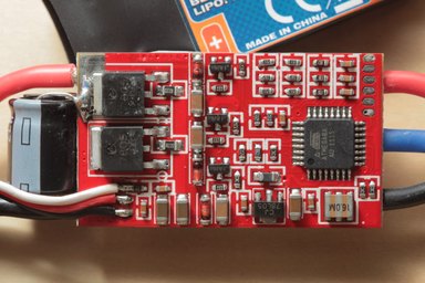
Finally, an improvement over the above is the all-N-channel layout with dedicated driving ICs for each phase. These are easily identified by there being three ICs instead of the discrete driving components such as NPN transistors. The circuits in these chips maintain a proper gate driving voltage for both high and low sides and can offer better switching times and protection against cross-conduction and input voltage drop-out. Dedicated FET-driving ICs are typically found on larger ESCs and those which support input voltages above ~16V (4S). Some ICs expect inverted high or low side inputs, indicated as a line above "LIN" or "HIN" in the datasheet.
The first step in identifying how an ESC is wired is to track down which MCU pins drive the MOSFETs that power the motor. For a three-phase H-bridge, there are 6 required pins. For this, you will likely want to print out or load up the pin layout for the MCU. You can find this typically at the start of the data sheet (for ATmega8, see this post).
Next, figure out what you want to call phase A, B, and C. This may be written on the ESC somewhere, or you may just have to chose one side as A and the other as C. It does not matter in the end, as long as you keep everything straight. (You may eventually wish to flip A and C such that if you are replacing stock software, the motor still spins in the same direction by default.)
For ESCs with dedicated driver ICs, identification of the pins is often quite simple, because no additional components between the driver IC inputs and the MCU outputs are required. Simply connect a multimeter in contunity mode (beeps when probes are touched together) to the two input pins on each driver IC, and try each of the pins at the MCU to figure out where they are routed. Check the MOSFET driver data sheet (commonly ir2101s or BL8003) for input pins, since you will also need to check if the input is inverted or not. Most often, the input pins are pins 2 and 3 (which are right next to pin 1 which is closest to the dot on the package). You can usually speed up the process by seating the probe such that it touches both pins and then sweep across the MCU package to find the two pins. Write down or mark each driver input pin number and the associated MCU pin.
For ESCs without dedicated driver ESCs, it is often easiest to start with the low-side FETs, since they may just be directly connected. There is usually a resistor which may be too high for a multimeter to notice continuity, but you can use an Ohm-meter to look for the path that should be under 200 Ohms. This can sometimes be tricky as the FETs are often on the other side of the ESC than the MCU. First, check which are the low-side FETs by seeing which group of FETs have a direct connection to the ground (the black battery wire) on their source pin. Then, measure resistance between the gate pin and each MCU pin. Write down the MCU pin as the low-side pin for that phase. Next, the high-side FETs (with a drain pin connected to the battery voltage, red wire) will need to be mapped back. However, these will be going through NPN transistors. You will need to first track to the collector pin of one of the three NPNs, and then track from the base of that NPN to the MCU pin.
With the FET pins identified, it may already be possible to find an existing software build that will work on the ESC. Even without identifying anything further, finding a match for FET pin configuration and inversion is typically enough to avoid fatal mishaps, even if it may not actually be able to drive a motor. You may wish to skip this step first just to check for possible existing software first. If it is not possible to find existing software, or if creating a new pin mapping file or software, continue here.
A brushless motor is driven by connecting one phase to battery voltage and another to ground, and stepping through each combination of two phases being connected this way such that the magnetic fields will rotate the motor. In each step, one of the phases is left "floating". For sensorless brushless ESCs, this phase is watched for motor back-EMF voltage to try to see where the motor is and determine when to advance to the next driving step. In order to do this, each phase must be connected to the MCU. The phases are usually with a resistor divider to ground so that the phase voltages do not exceed the MCU electrical rating. Depending on drive technique and implementation, this may only take three MCU pins. In most cases, a "neutral" pin is also needed which is either fed from the motor or emulated through a resistor star between each phase.
For ATmega8-based ESCs, hardware options are limited for which pins can succcessfully be used to sense the motor phases. The ADC is too slow for absolute voltage measurements of each phase, so the comparator is used instead, and four pins are required. Since the comparator will be used to compare neutral against each phase voltage, and the neutral pin typically must be connected to AIN0, which is fixed as the positive comparator input. The negative comparator input is by default on AIN1, but is switchable by the ADC MUX in the ATmega8 to any ADC pin. So, the search can be limited to only these pins.
Measure the resistance between each motor output wire and all of the possible MCU pins. There should be one pin that has the lowest resistance for each motor phase. There should also be equal resistance from the neutral pin, if applicable, and each of the sense pins. Write down each of the pins for each phase and neutral.
Almost all RC brushless ESCs expect pulse-width modulation signalling from a radio receiver or flight control board. This pin is commonly connected directly or with a light resistor to a pin that can cause interrupts on the MCU. On ATmega8-based ESCs, the options are typically limited to the INT0 (PD2), INT1 (PD3), or ICP (PB0) pins. INT0/PD2 is most commonly seen.
Some boards will have opto-isolation on the input pin. The simplest way to connect the opto-isolator typically involves inverting the input, so these ones will measure high at the MCU when the PWM input pin is low at the connector, and vice versa. These are easily identified as a four-legged opto-isolator component and a transistor. However, some lines of ESCs which wish to use common software across various board versions may implement the inversion but not the opto-isolation, so look for a transistor connected to the PWM input pin. Write down the pin this is connected to, and if it appears to be inverted.
Depending on the ESC software, there may be various shortcuts to most quickly find if the board is supported. For example, comparatively few boards use inverted PWM input, meaning the rest can be excluded if this is required.
Different software will have different ways of describing the pin configuration, but there are three main pieces. The FET driving pins and inversion are most important. In many cases, "P" will be used to denote high-side FETs even on boards with all-N-channel MOSFETs.
For Simon Kirby's "tgy" software, a format similar to Bernhard Konze (quax)'s layout is used. Each ".inc" file in the tree defines a board configuration. The file starts with some on/off configurations for input types and inversions. A value of 0 means off, 1 means on, and (a special case) 2 means on and inverted. For example, the most common board type will have USE_INT0=1, whereas inverted input boards will have USE_INT0=2. The FET pins are listed per PORT (B, C, D), and inverted status is "defined" in several places: both in the INIT_Px values (initial port values) and in the macros to toggle FETs on and off. Inverted FET drive pins will use clear instructions such as "cbi" instead of set instructions such as "sbi" to turn on a FET, and vice versa. For examples, see tgy.inc and tp_nfet.inc. Finally, switching sense pins are implemented as macros.
There can be a lot of board types to check, and this can be a daunting task. It may be easier to start with an existing random board configuration file and adjust the FET pins to match your board based on your findings. Then, check to see if this configuration matches the file you started with or any other file. If possible, start with a file listed elsewhere on the Internet, such as in the ESC compatibility spreadsheet.
This will depend on the software used.
For Simon Kirby's "tgy" software, add the .inc file name where else other .inc file names occur in Makefile and tgy.asm, then run "make". In Windows, you may need to use AVR Studio and explicitly specify your include file to build it.
When flashing and testing any ESC, power the ESC from a current-limited supply. An inexpensive solution if a current-limited supply is not available is to use a small automotive light-bulb in series with a higher-current source. This should prevent damage to components.