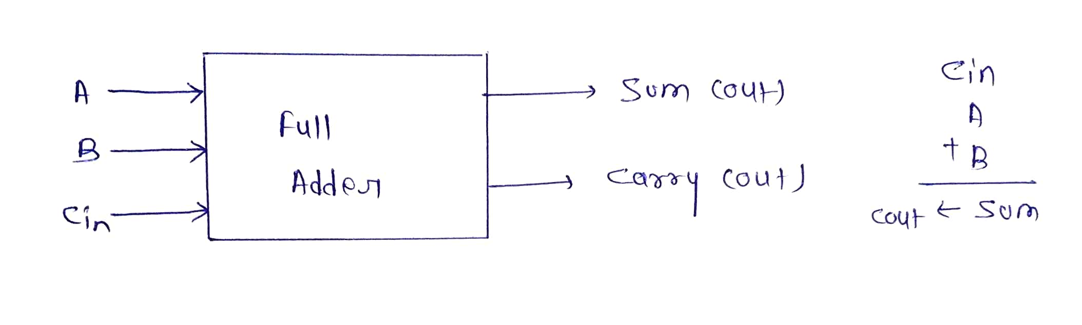
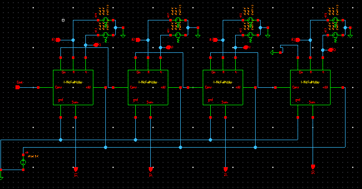
In this paper design of 4-Bit ripple carry adder is proposed using a CMOS full adder cell. Multiple full adder circuits can be cascaded in parallel to add an N-bit number .For N-bit parallel adder , there must be N number of full adder circuits. A ripple carry adder is a logic circuit in which the carry out of each full adder is the carry in of the succeeding next most significant full adder.To understand the working of a ripple carry adder completely , you need to have a look at the full adder too.Full adder is a logic circuit that add two input operand bits plus a carry in bit and output a carry out bit and sum bit. I have implemented Ripple Carry Adder with the help of CMOS Full adder.
• Synopsys Custom Compiler:
The Synopsys Custom Compiler™ design environment is a modern solution for full-custom analog, custom digital, and mixed-signal IC design. As the heart of the Synopsys Custom Design Platform, Custom Compiler provides design entry, simulation management and analysis, and custom layout editing features. This tool was used to design the circuit on a transistor level.
• Synopsys Primewave:
PrimeWave™ Design Environment is a comprehensive and flexible environment for simulation setup and analysis of analog, RF, mixed-signal design, custom-digital and memory designs within the Synopsys Custom Design Platform. This tool helped in various types of simulations of the above designed circuit.
• Synopsys 28nm PDK:
The Synopsys 28nm Process Design Kit(PDK) was used in creation and simulation of the above designed circuit.
4 full adder circuits can be cascaded in parallel to add an 4-bit number. For an 4-bit parallel adder, there must be 4 full adder circuits. A ripple carry adder is a logic circuit in which the carry-out of each full adder is the carry-in of the succeeding next most significant full adder. It is called a ripple carry adder because each carry bit gets rippled into the next stage. In a ripple carry adder the sum and carry out bits of any half adder stage is not valid until the carry in of that stage occurs.Propagation delays inside the logic circuitry is the reason behind this. Propagation delay is time elapsed between the application of an input and occurance of the corresponding output. Consider a NOT gate, When the input is “0” the output will be “1” and vice versa. The time taken for the NOT gate’s output to become “0” after the application of logic “1” to the NOT gate’s input is the propagation delay here. Similarly the carry propagation delay is the time elapsed between the application of the carry in signal and the occurrence of the carry out (Cout) signal.To understand the working of full adder completely , you need to have a look at the full adder too. Full adder is a logic circuit that add two input operand bits plus carry out bit and sum bit. A full adder can be made by two half adder circuit together .Alternatively the full adder can be made using NAND or NOR logic.Below the schematic diagram of Full Adder to add 1-Bit.
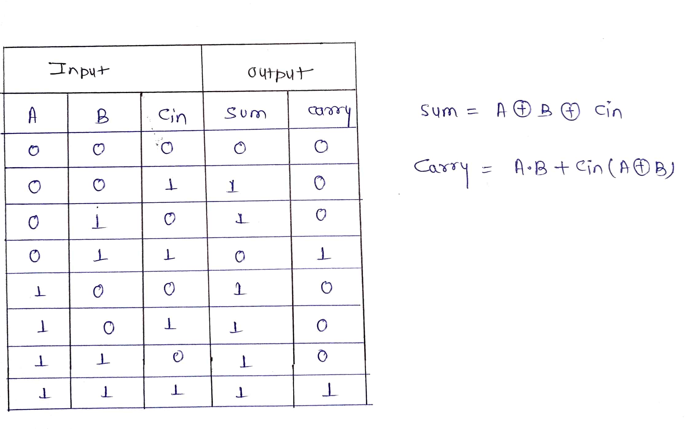
To understand the working of ripple carry adder completely, you need to have a look at the Full Adder too. Full Adder is a Logic circuit that add two input operand bits plus a Carry in bit and output a Cout bit and Sum out bit. The Sum out (Sout) of a full adder is the Xor of input input operand bits A,B and the carry in (Cin) bit. truth table and schematic of a 1-bit full adder is shown below. there is a simple trick to find result of a full adder . consider the second last row of the truth table, here the operand are 1,1,0 ie (A,B,Cin). Add them together ie 1+1+0=10. In binary system , the number order is 0,1,10,11.......and so the result of 1+1+0 is 10 just like we get 1+1+0=2 in decimal system. 2 in the decimal system corresponds to 10 in the binary sysyetm.
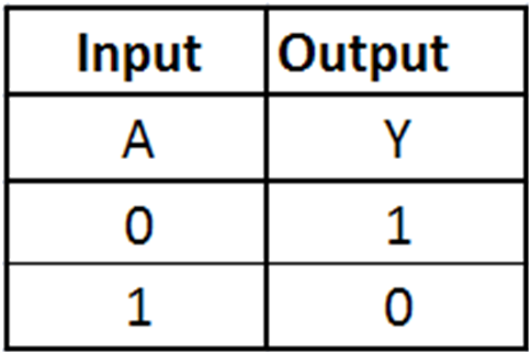
A basic Binary Adder circuit can be made from standard AND and XOR gates allowing us to "add" together two single bit binary number, A and B.


####Truth table of Not gate


* Generated for: PrimeSim
* Design library name: Ripple_Carry_Adder
* Design cell name: ripple_carry_adder
* Design view name: schematic
.lib '/PDK/SAED_PDK32nm/hspice/saed32nm.lib' TT
*Custom Compiler Version S-2021.09
*Thu Feb 24 12:31:28 2022
.global gnd!
********************************************************************************
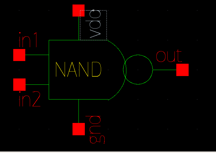
* Library : NAND_GATE
* Cell : nand_gate
* View : schematic
* View Search List : hspice hspiceD schematic spice veriloga
* View Stop List : hspice hspiceD
********************************************************************************
.subckt nand_gate gnd_1 in1 in2 out vdd
xm1 net5 in2 gnd_1 gnd_1 n105 w=0.1u l=0.03u nf=1 m=1
xm0 out in1 net5 net5 n105 w=0.1u l=0.03u nf=1 m=1
xm3 out in2 vdd vdd p105 w=0.1u l=0.03u nf=1 m=1
xm2 out in1 vdd vdd p105 w=0.1u l=0.03u nf=1 m=1
.ends nand_gate
********************************************************************************
* Library : Inverter_ghanshu
* Cell : inverter
* View : schematic
* View Search List : hspice hspiceD schematic spice veriloga
* View Stop List : hspice hspiceD
********************************************************************************
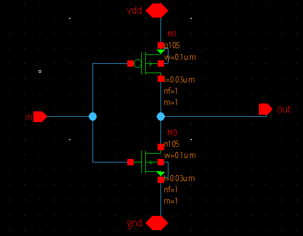
.subckt inverter gnd_1 in out vdd
xm0 out in gnd_1 gnd_1 n105 w=0.1u l=0.03u nf=1 m=1
xm1 out in vdd vdd p105 w=0.1u l=0.03u nf=1 m=1
.ends inverter
********************************************************************************
* Library : XOR_GATE
* Cell : xor_gate
* View : schematic
* View Search List : hspice hspiceD schematic spice veriloga
* View Stop List : hspice hspiceD
********************************************************************************
.subckt xor_gate a b gnd_1 out vdd
xm3 out a net15 net15 n105 w=0.1u l=0.03u nf=1 m=1
xm2 out net35 net11 net11 n105 w=0.1u l=0.03u nf=1 m=1
xm1 net15 b gnd_1 gnd_1 n105 w=0.1u l=0.03u nf=1 m=1
xm0 net11 net39 gnd_1 gnd_1 n105 w=0.1u l=0.03u nf=1 m=1
xm7 net33 b vdd vdd p105 w=0.1u l=0.03u nf=1 m=1
xm6 net33 a vdd vdd p105 w=0.1u l=0.03u nf=1 m=1
xm5 out net39 net33 net33 p105 w=0.1u l=0.03u nf=1 m=1
xm4 out net35 net33 net33 p105 w=0.1u l=0.03u nf=1 m=1
xi10 gnd_1 b net39 vdd inverter
xi9 gnd_1 a net35 vdd inverter
.ends xor_gate
********************************************************************************
* Library : XNOR_GATE
* Cell : xor_gate
* View : schematic
* View Search List : hspice hspiceD schematic spice veriloga
* View Stop List : hspice hspiceD
********************************************************************************
.subckt xor_gate_1 a b out gnd_1 vdd
xi0 a b gnd_1 net9 vdd xor_gate
xi1 gnd_1 net9 out vdd inverter
.ends xor_gate_1
********************************************************************************
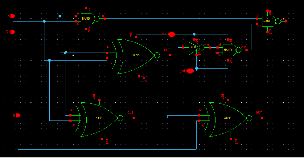
* Library : 1_Bit_Full_Adder
* Cell : full_Adder
* View : schematic
* View Search List : hspice hspiceD schematic spice veriloga
* View Stop List : hspice hspiceD
********************************************************************************
.subckt full_adder a b carry cin sum gnd_1 vdd
xi2 gnd_1 net31 b net11 vdd nand_gate
xi1 gnd_1 net36 net11 carry vdd nand_gate
xi0 gnd_1 a cin net36 vdd nand_gate
xi5 net29 b sum gnd_1 vdd xor_gate_1
xi4 a cin net29 gnd_1 vdd xor_gate_1
xi3 a cin net34 gnd_1 vdd xor_gate_1
xi6 gnd_1 net34 net31 vdd inverter
.ends full_adder
********************************************************************************
* Library : Ripple_Carry_Adder
* Cell : ripple_carry_adder
* View : schematic
* View Search List : hspice hspiceD schematic spice veriloga
* View Stop List : hspice hspiceD
********************************************************************************
xi3 a3 b3 cout net26 s3 gnd! net29 full_adder
xi2 a2 b2 net26 net19 s2 gnd! net29 full_adder
xi1 a1 b1 net19 net12 s1 gnd! net29 full_adder
xi0 a0 b0 net12 gnd! s0 gnd! net29 full_adder
v4 net29 gnd! dc=1.8
v14 b3 gnd! dc=0 pulse ( 1 0 0 0.1u 0.1u 5u 40u )
v13 a3 gnd! dc=0 pulse ( 0 1 0 0.1u 0.1u 5u 40u )
v12 b2 gnd! dc=0 pulse ( 0 1 0 0.1u 0.1u 5u 40u )
v11 a2 gnd! dc=0 pulse ( 0 1 0 0.1u 0.1u 5u 40u )
v18 b0 gnd! dc=0 pulse ( 0 1 0 0.1u 0.1u 5u 40u )
v17 a0 gnd! dc=0 pulse ( 0 1 0 0.1u 0.1u 5u 10u )
v15 a1 gnd! dc=0 pulse ( 1 0 0 0.1u 0.1u 5u 40u )
v16 b1 gnd! dc=0 pulse ( 0 1 0 0.1u 0.1u 5u 40u )
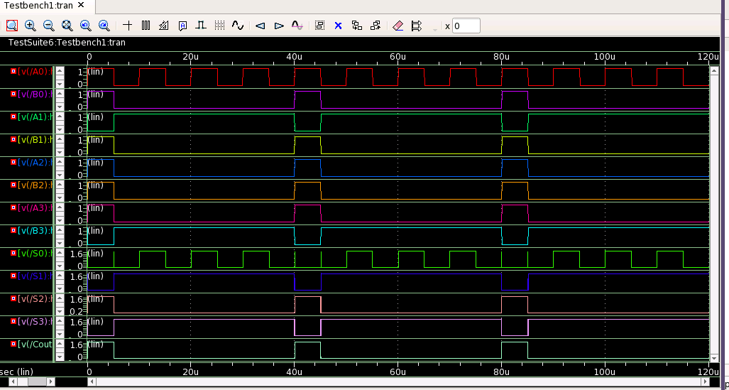
.tran '1u' '120u' name=tran
.option primesim_remove_probe_prefix = 0
.probe v(*) i(*) level=1
.probe tran v(a0) v(a1) v(a2) v(a3) v(b0) v(b1) v(b2) v(b3) v(cout) v(s0) v(s1)
+ v(s2) v(s3)
.temp 25
.option primesim_output=wdf
.option parhier = LOCAL
.end• Ghanshyam Verma, M.Tech(VLSI), IIIT–Naya Raipur, Atal Nagar – 493661
• Cloud Based Analog IC Design Hackathon
• Synopsys India
• VLSI System Design (VSD) Corp. Pvt. Ltd India
[1]Radha, S., et al. "Floor planning of 16 bit counter design for health care applications using 180nm technology in cadence tool." 2018 Second International Conference on Electronics, Communication and Aerospace Technology (ICECA). IEEE, 2018.