This repository presents the design of 4_bit_adder_subtractor implemented using Synopsis Custom Compiler on 32nm CMOS Technology.
- Abstract
- Synopsys Custom Compiler Tool Details
- Reference Circuit details
- Reference Circuit Diagram
- Reference WaveForm
- Synopsys Simulations
- Schematics and Symbols
- Vdd and Vgs values for MOSFETS
- Transient settings
- Testbench
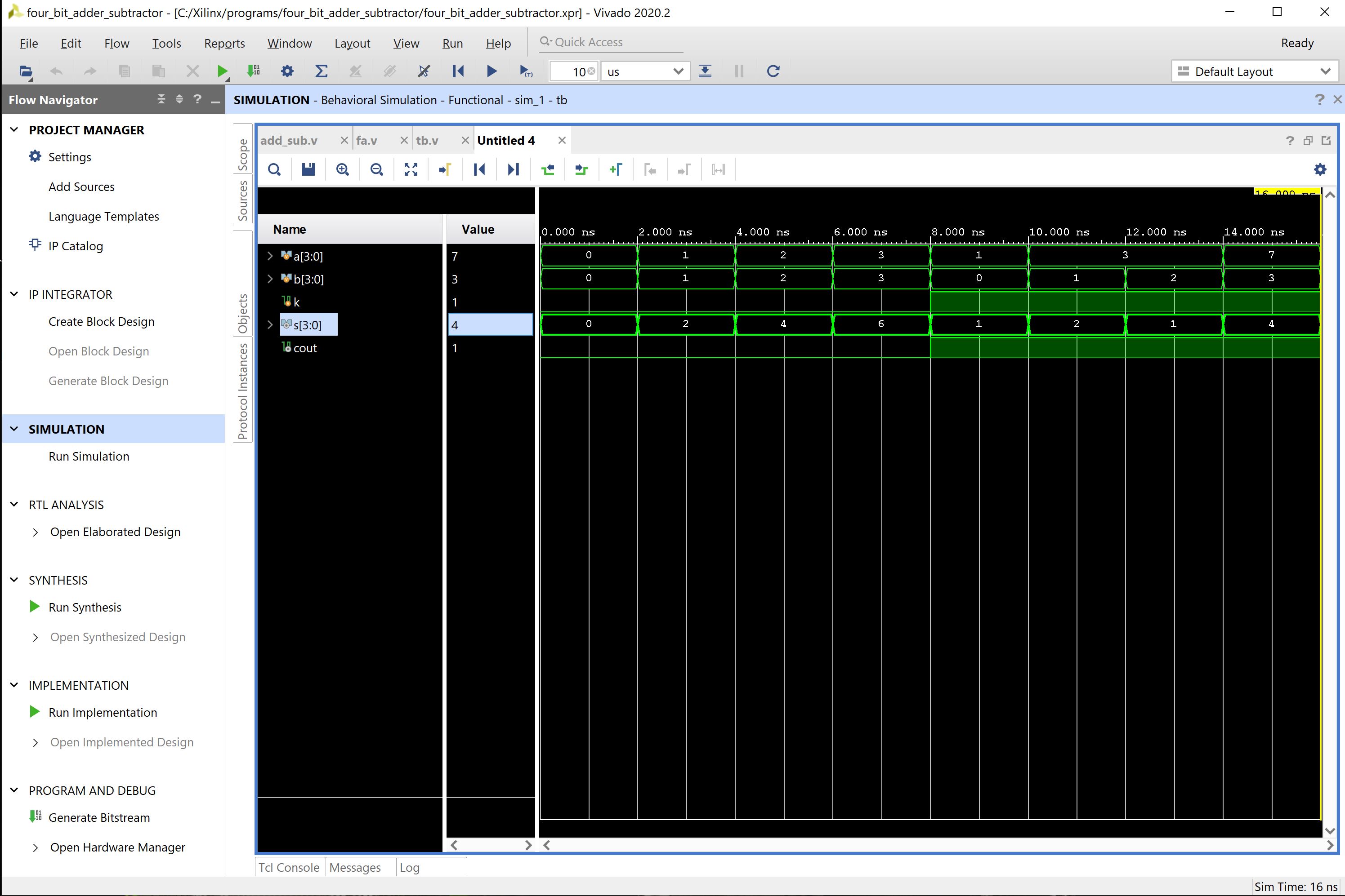
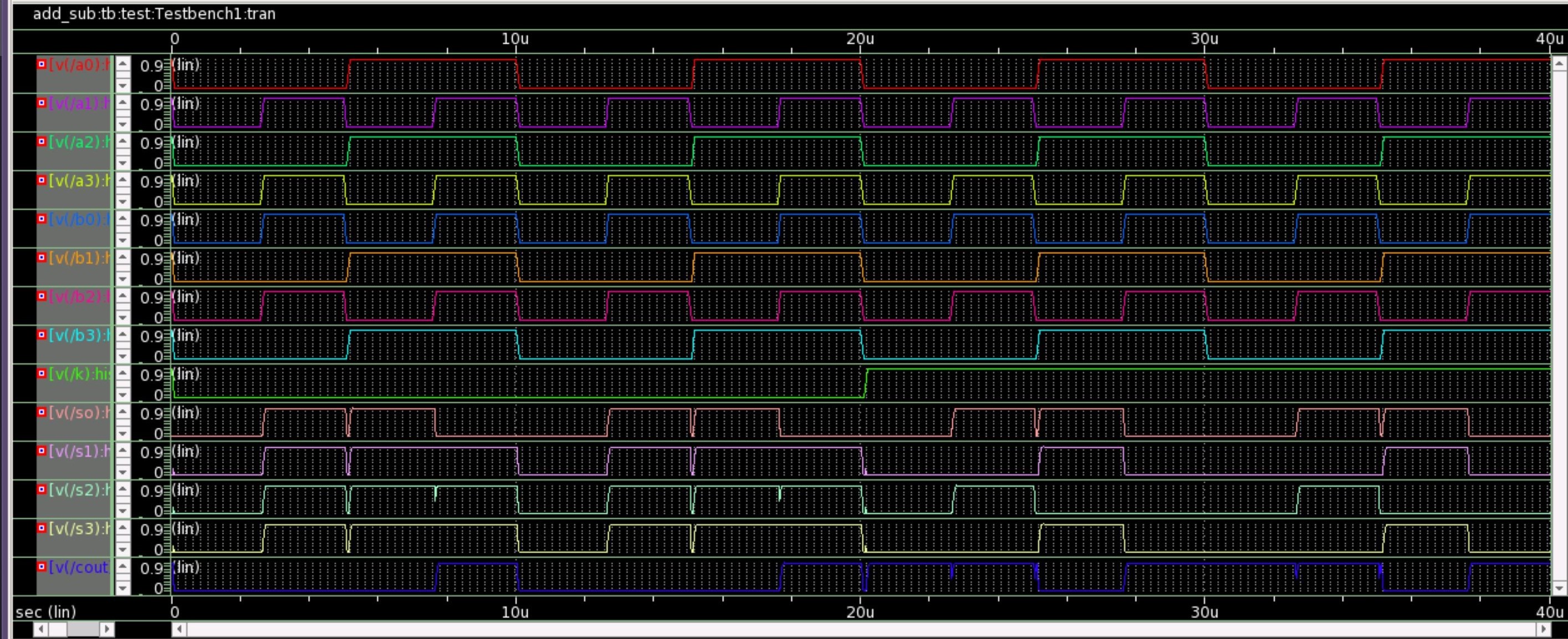
- Simulated Waveform
- Netlist
- Conclusion
- Acknowledgement
- References
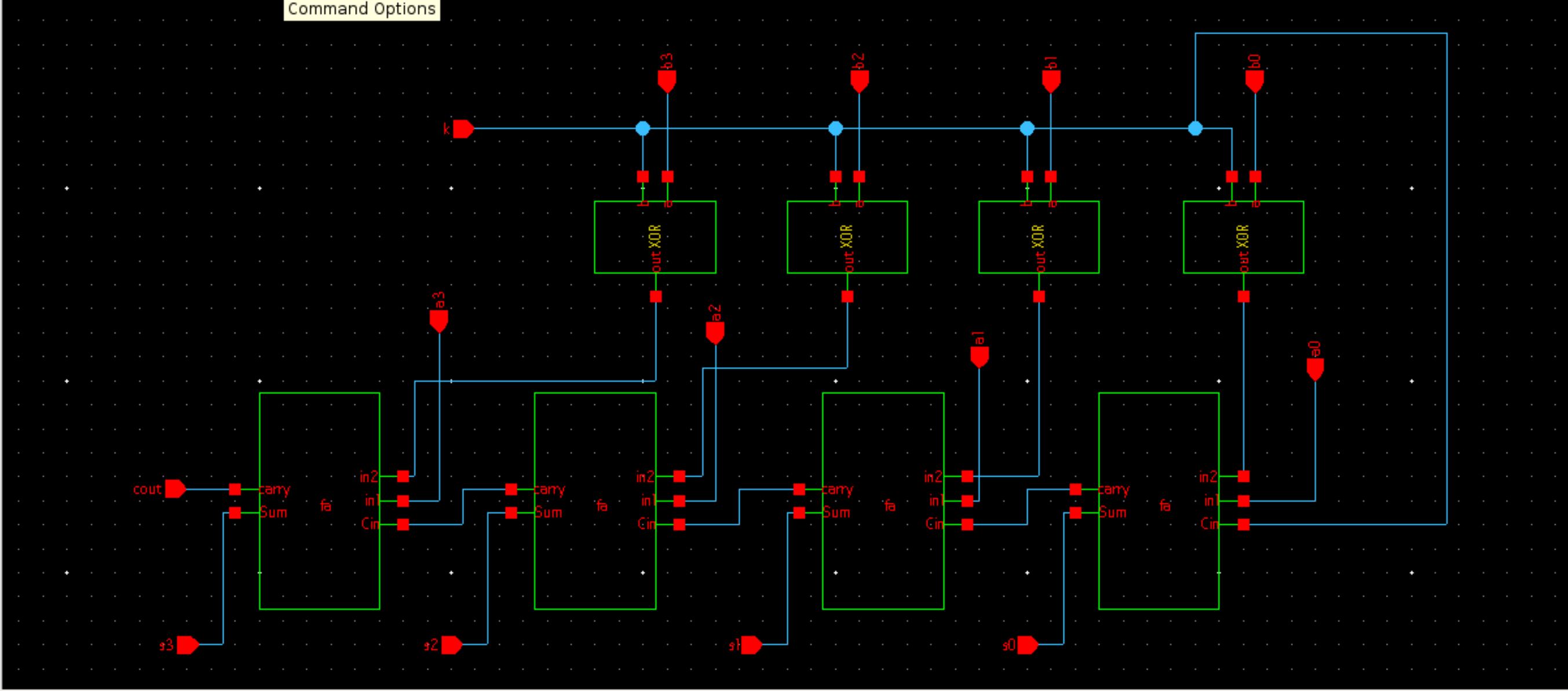
The need to have hardware support for binary arithmetic is increasing in recent years because of the growth in the Binary data processing in commercial, financial and internet based applications. In this paper you will go through A binary 4bit_Adder-Subtractor. It is a combinational circuit which is capable of performing binary addition and subtraction in one circuitry. The operation mode can be selected using control signal, control singal will also be taken as input to the 1st stage full adder. This circuitry is a combination of logic gates like and, or, xor gates.The major principle followed in this circutry is take from the ripple carry adder circuitry in which carry out of the previous stage full adder is given as input carry to the next full adder.This circuit majorly required the prerequisite knowledge on XOR gate, because by which we are performing 2'complement on one set of input data to perform subtraction operation.
The Synopsys Custom Compiler™ design environment is a modern solution for full-custom analog, custom digital, and mixed-signal IC design. As the heart of the Synopsys Custom Design Platform, Custom Compiler provides design entry, simulation management and analysis, and custom layout editing features. It delivers industry-leading productivity, performance, and ease-of-use while remaining easy to adopt for users of legacy tools.

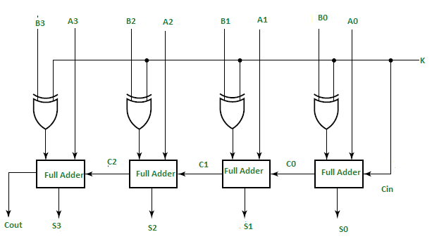
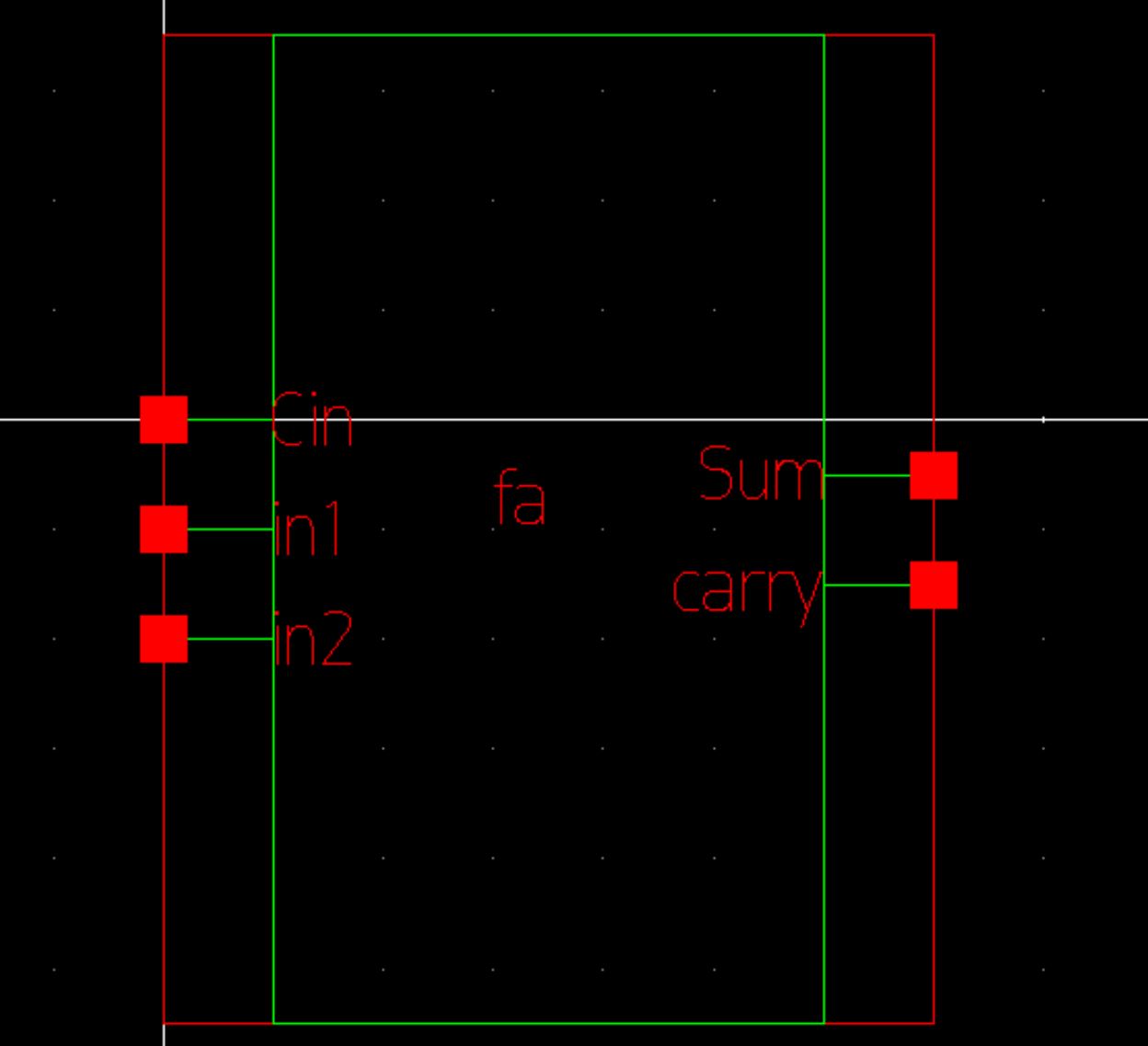
- The circuit shown in the reference diagram (a) has total of 9 input ports, In which a0 to a3 and b0 to b3 are the binary inputs, K is the control signal input which decides the mode of operation. Cin, c0 to c2 are the internal wires. S0 to s3 are the output ports with gives the addition or subtraction value depending on the selected mode and cout is also a output port which may give carry in case of addition and borrow in case of difference . As it is 4 bit adder-subtractor we are using four xor gates and 4 one bit full adders. The diagram (b) show the internal circuitry of the one bit full adder which is having 3 input ports(a,b,cin) and 2(cout,sum) output ports.
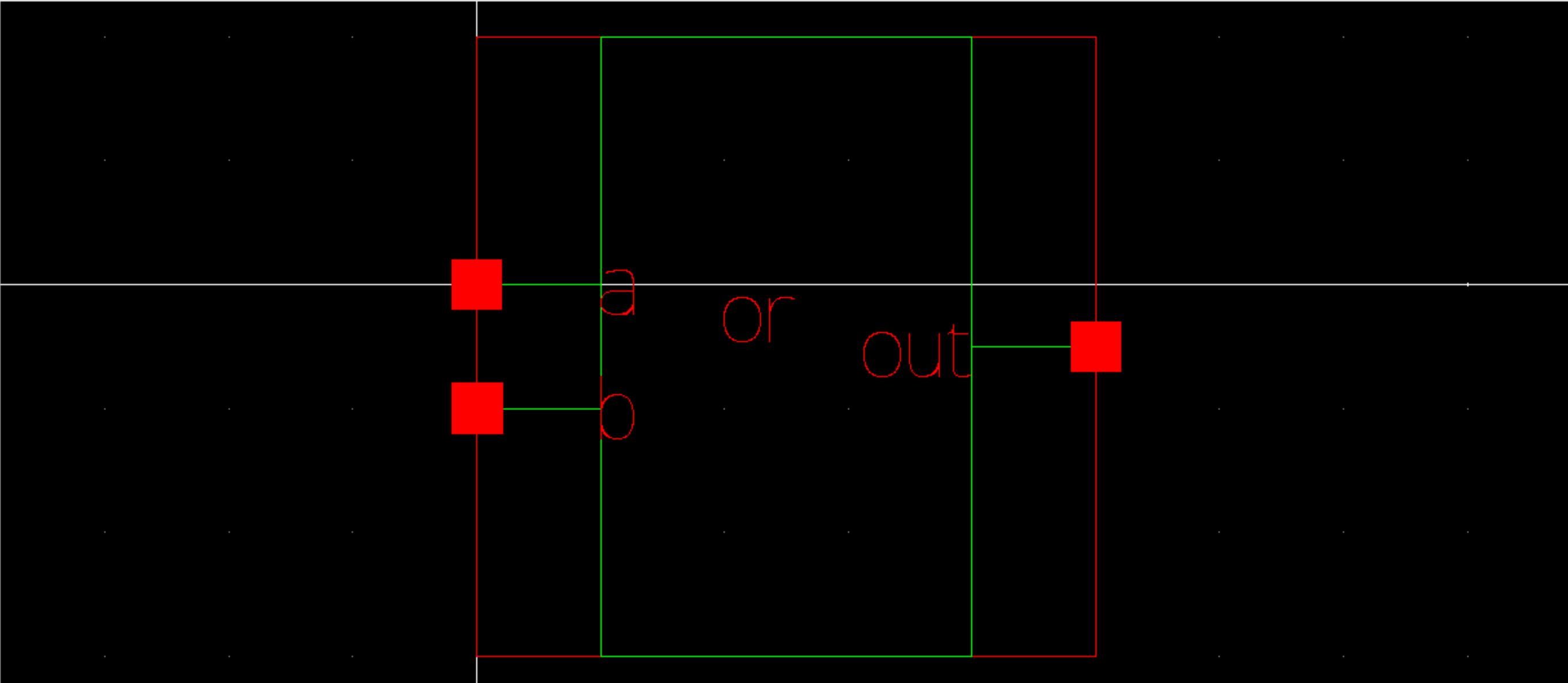
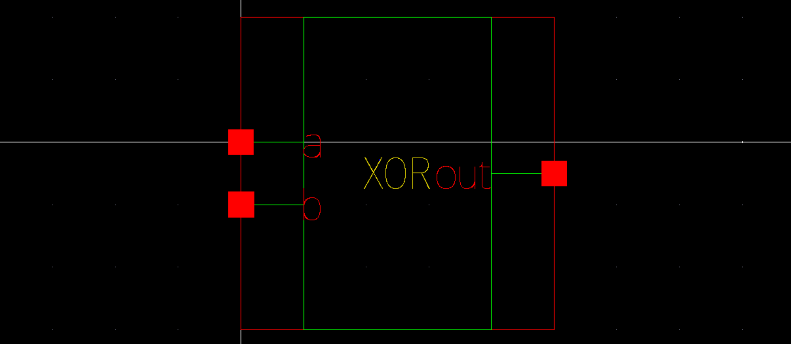
- The gates used in the diagram a,b are:-
- xor
- or
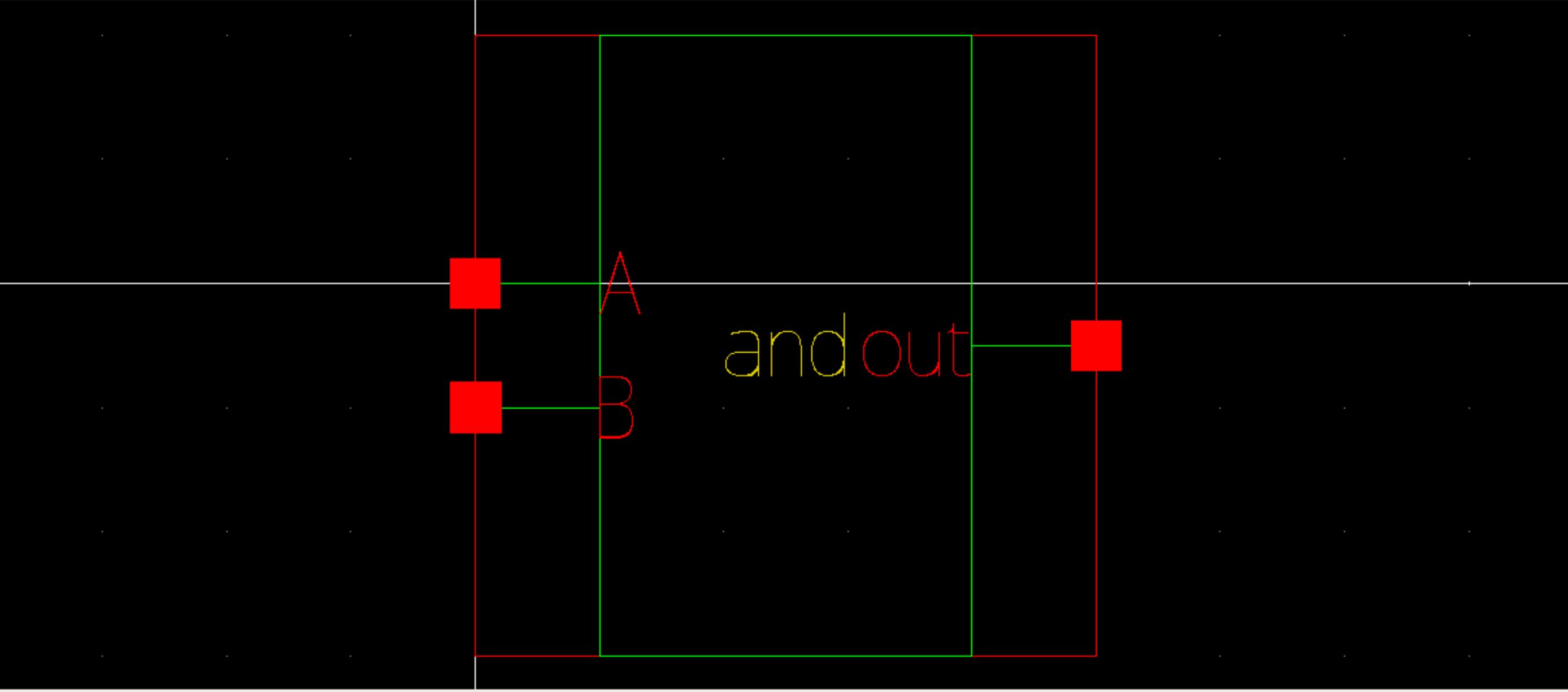
- and
- boolean equations for full adder:-
- SUM=A⊕B⊕C
- CARRY=A.B + A.Cin + B.Cin
- boolean equations for full subtractor:-
- DIFFERENCE =A⊕B C⊕
- BORROW =A’.B + A’.Cin + B.Cin
- Main Circuit:-
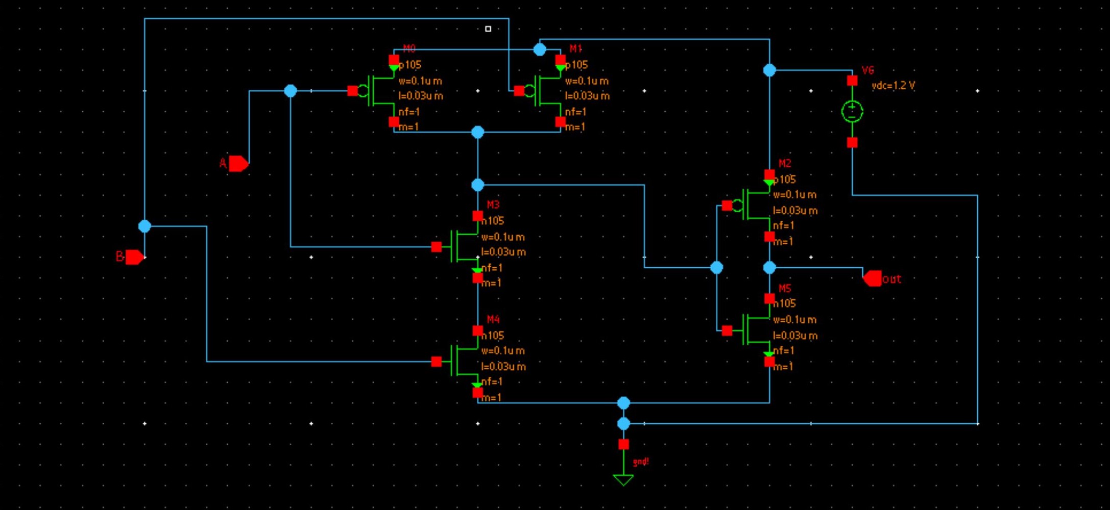
- Full adder:-

- and gate:-
- Or gate:-

- Xor gate:-

- Full Adder:-

- Main Circuit:-
- Vdd:-
- Vgs:-

* Generated for: PrimeSim
* Design library name: add_sub
* Design cell name: tb
* Design view name: schematic
.lib 'saed32nm.lib' TT
*Custom Compiler Version S-2021.09
*Tue Feb 22 16:09:10 2022
.global gnd! vdd!
********************************************************************************
* Library : add_sub
* Cell : or
* View : schematic
* View Search List : hspice hspiceD schematic spice veriloga
* View Stop List : hspice hspiceD
subckt or a b out vt_bulk_n_gnd! vt_bulk_p_vdd!
xm8 net30 a net12 vt_bulk_p_vdd! p105 w=0.1u l=0.03u nf=1 m=1
xm6 out net47 net12 vt_bulk_p_vdd! p105 w=0.1u l=0.03u nf=1 m=1
xm3 net18 b net12 vt_bulk_p_vdd! p105 w=0.1u l=0.03u nf=1 m=1
xm4 net47 net4 net18 vt_bulk_p_vdd! p105 w=0.1u l=0.03u nf=1 m=1
xm5 net47 a net18 vt_bulk_p_vdd! p105 w=0.1u l=0.03u nf=1 m=1
xm2 net18 net30 net12 vt_bulk_p_vdd! p105 w=0.1u l=0.03u nf=1 m=1
xm0 net4 b net12 vt_bulk_p_vdd! p105 w=0.1u l=0.03u nf=1 m=1
xm14 out net47 gnd! vt_bulk_n_gnd! n105 w=0.1u l=0.03u nf=1 m=1
xm13 net42 b gnd! vt_bulk_n_gnd! n105 w=0.1u l=0.03u nf=1 m=1
xm12 net47 net30 net42 vt_bulk_n_gnd! n105 w=0.1u l=0.03u nf=1 m=1
xm11 net49 a gnd! vt_bulk_n_gnd! n105 w=0.1u l=0.03u nf=1 m=1
xm10 net47 net4 net49 vt_bulk_n_gnd! n105 w=0.1u l=0.03u nf=1 m=1
xm9 net30 a gnd! vt_bulk_n_gnd! n105 w=0.1u l=0.03u nf=1 m=1
xm1 net4 b gnd! vt_bulk_n_gnd! n105 w=0.1u l=0.03u nf=1 m=1
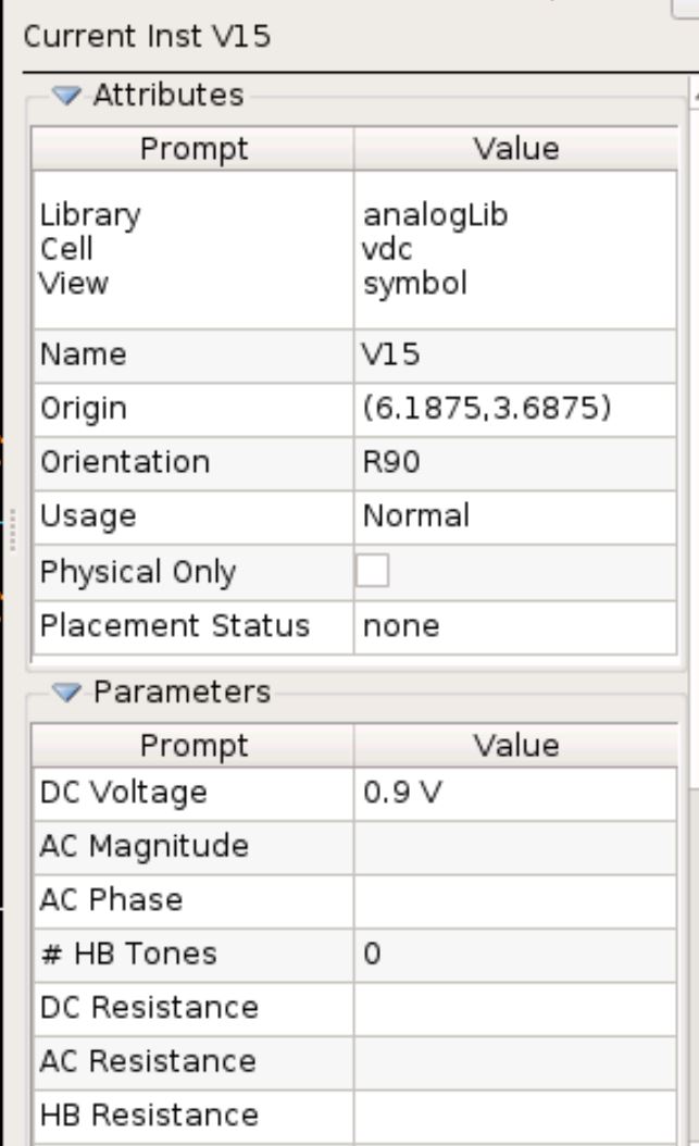
v15 net12 gnd! dc=0.9
.ends or
********************************************************************************
* Library : add_sub
* Cell : and
* View : schematic
* View Search List : hspice hspiceD schematic spice veriloga
* View Stop List : hspice hspiceD
subckt and a b out vt_bulk_n_gnd! vt_bulk_p_vdd!
xm2 out net18 net20 vt_bulk_p_vdd! p105 w=0.1u l=0.03u nf=1 m=1
xm1 net18 b net20 vt_bulk_p_vdd! p105 w=0.1u l=0.03u nf=1 m=1
xm0 net18 a net20 vt_bulk_p_vdd! p105 w=0.1u l=0.03u nf=1 m=1
xm5 out net18 gnd! vt_bulk_n_gnd! n105 w=0.1u l=0.03u nf=1 m=1
xm4 net13 b gnd! vt_bulk_n_gnd! n105 w=0.1u l=0.03u nf=1 m=1
xm3 net18 a net13 vt_bulk_n_gnd! n105 w=0.1u l=0.03u nf=1 m=1
v6 net20 gnd! dc=1.2
.ends and
********************************************************************************
* Library : add_sub
* Cell : xor
* View : schematic
* View Search List : hspice hspiceD schematic spice veriloga
* View Stop List : hspice hspiceD
subckt xor a b out vt_bulk_n_gnd! vt_bulk_p_vdd!
xm2 out net19 net26 vt_bulk_p_vdd! p105 w=0.1u l=0.03u nf=1 m=1
xm1 net19 b net4 vt_bulk_p_vdd! p105 w=0.1u l=0.03u nf=1 m=1
xm0 net4 a net26 vt_bulk_p_vdd! p105 w=0.1u l=0.03u nf=1 m=1
xm5 out net19 gnd! vt_bulk_n_gnd! n105 w=0.1u l=0.03u nf=1 m=1
xm4 net19 a gnd! vt_bulk_n_gnd! n105 w=0.1u l=0.03u nf=1 m=1
xm3 net19 b gnd! vt_bulk_n_gnd! n105 w=0.1u l=0.03u nf=1 m=1
v8 net26 gnd! dc=0.9
.ends xor
********************************************************************************
* Library : add_sub
* Cell : adder
* View : schematic
* View Search List : hspice hspiceD schematic spice veriloga
* View Stop List : hspice hspiceD
subckt adder cin sum carry in1 in2 vt_bulk_n_gnd! vt_bulk_p_vdd!
xi2 net23 cin sum vt_bulk_n_gnd! vt_bulk_p_vdd! or
xi1 in1 in2 net23 vt_bulk_n_gnd! vt_bulk_p_vdd! or
xi4 in1 in2 net18 vt_bulk_n_gnd! vt_bulk_p_vdd! and
xi3 cin net23 net17 vt_bulk_n_gnd! vt_bulk_p_vdd! and
xi5 net17 net18 carry vt_bulk_n_gnd! vt_bulk_p_vdd! xor
.ends adder
********************************************************************************
* Library : add_sub
* Cell : adder_subtractor
* View : schematic
* View Search List : hspice hspiceD schematic spice veriloga
* View Stop List : hspice hspiceD
subckt adder_subtractor a0 a1 a2 a3 b0 b1 b2 b3 cout k s0 s1 s2 s3
+ vt_bulk_n_gnd! vt_bulk_p_vdd!
xi3 b0 k net13 vt_bulk_n_gnd! vt_bulk_p_vdd! or
xi2 b1 k net18 vt_bulk_n_gnd! vt_bulk_p_vdd! or
xi1 b2 k net23 vt_bulk_n_gnd! vt_bulk_p_vdd! or
xi0 b3 k net28 vt_bulk_n_gnd! vt_bulk_p_vdd! or
xi7 net30 s3 cout a3 net28 vt_bulk_n_gnd! vt_bulk_p_vdd! adder
xi6 net25 s2 net30 a2 net23 vt_bulk_n_gnd! vt_bulk_p_vdd! adder
xi5 net20 s1 net25 a1 net18 vt_bulk_n_gnd! vt_bulk_p_vdd! adder
xi4 k s0 net20 a0 net13 vt_bulk_n_gnd! vt_bulk_p_vdd! adder
.ends adder_subtractor
********************************************************************************
* Library : add_sub
* Cell : tb
* View : schematic
* View Search List : hspice hspiceD schematic spice veriloga
* View Stop List : hspice hspiceD
v36 a3 gnd! dc=0 pulse ( 0.9 0 0 0.1u 0.1u 2.5u 5u )
v35 a2 gnd! dc=0 pulse ( 0.9 0 0 0.1u 0.1u 5u 10u )
v34 b0 gnd! dc=0 pulse ( 0.9 0 0 0.1u 0.1u 2.5u 5u )
v33 b1 gnd! dc=0 pulse ( 0.9 0 0 0.1u 0.1u 5u 10u )
v32 b2 gnd! dc=0 pulse ( 0.9 0 0 0.1u 0.1u 2.5u 5u )
v31 b3 gnd! dc=0 pulse ( 0.9 0 0 0.1u 0.1u 5u 10u )
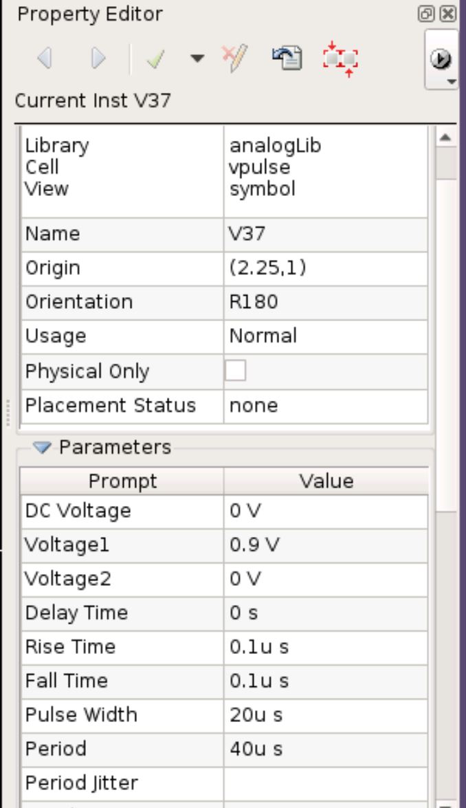
v37 k gnd! dc=0 pulse ( 0.9 0 0 0.1u 0.1u 20u 40u )
v16 a1 gnd! dc=0 pulse ( 0.9 0 0 0.1u 0.1u 2.5u 5u )
v8 a0 gnd! dc=0 pulse ( 0.9 0 0 0.1u 0.1u 5u 10u )
c26 cout gnd! c=1p
c21 so gnd! c=1p
c23 s1 gnd! c=1p
c24 s2 gnd! c=1p
c25 s3 gnd! c=1p
xi19 a0 a1 a2 a3 b0 b1 b2 b3 cout k so s1 s2 s3 gnd! vdd! adder_subtractor
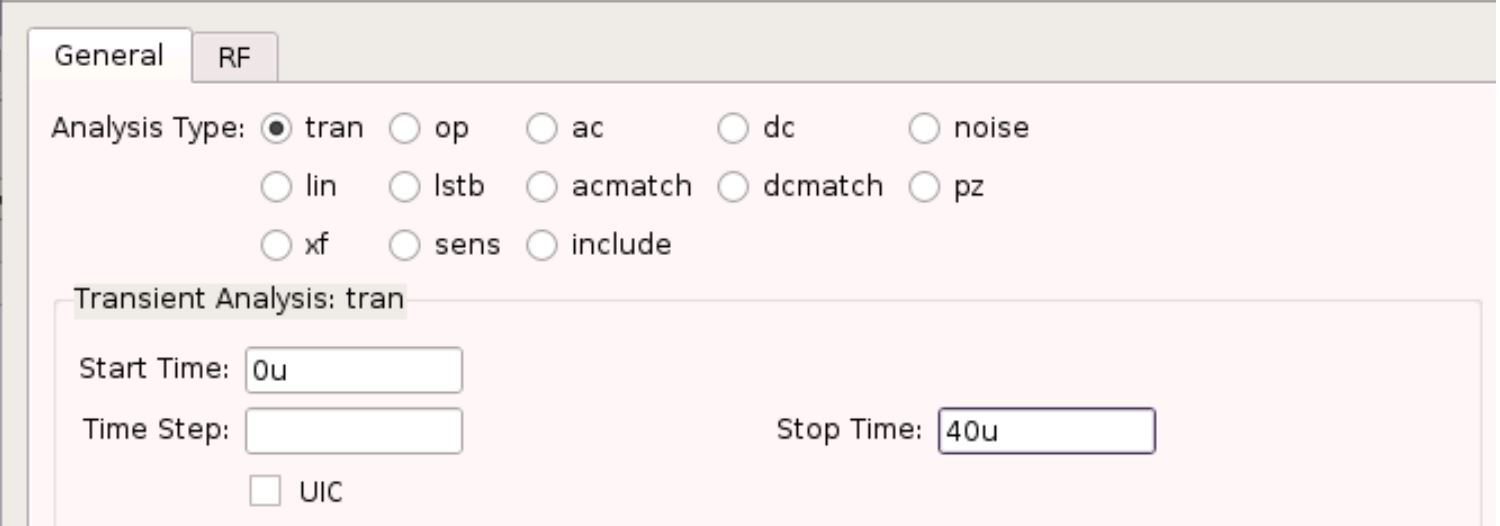
.tran '0.001*(40u-0u)' '40u' start=0u name=tran
.option primesim_remove_probe_prefix = 0
.probe v(*) i(*) level=1\
.probe tran v(a0) v(a1) v(a2) v(a3) v(b0) v(b1) v(b2) v(b3) v(cout) v(k) v(s1)
+ v(s2) v(s3) v(so)
.temp 25
.option primesim_output=wdf
.option parhier = LOCAL
.end
- We can reduce the use of multiple hardware resources required to make 4-bit full adder separately and another 4-bit full subtractor.
- By just using the control signal we can which between two modes adder and subtractor.
- With this design we can make N-bit adder_subtractor.
- 1.Cloud Based Analog IC Design Hackathon
- 2.Synopsys India
- 3.VLSI System Design (VSD) Corp. Pvt. Ltd India
- 4.Kunal Ghosh, Co-founder, VSD Corp. Pvt. Ltd.
- 5.Chinmay panda, IIT Hyderabad
- 6.Sameer Durgoji, NIT Karnataka