- The purpose of this project is to design a 4-bit Johnson Counter with Ring Oscillator using an Opensource EDA Tool called eSim, and Makerchip software and SKY130nm PDK technology.
- To explore the project, you can git clone using the command: git clone https://github.com/RadhaKulkarni26/4-bit-Johnson-Counter-with-Ring-Oscillator-using-SKY130nm-PDK.git
- INTRODUCTION
- WHAT ARE MIXED SIGNAL CIRCUITS?
- WHAT IS VERILOG AND TL-VERILOG?
- INSTALLATION OF TOOLS
- CIRCUIT DESIGN
- REFERENCE CIRCUIT DIAGRAM
- Digital Block Diagram
- Analog Block Diagram
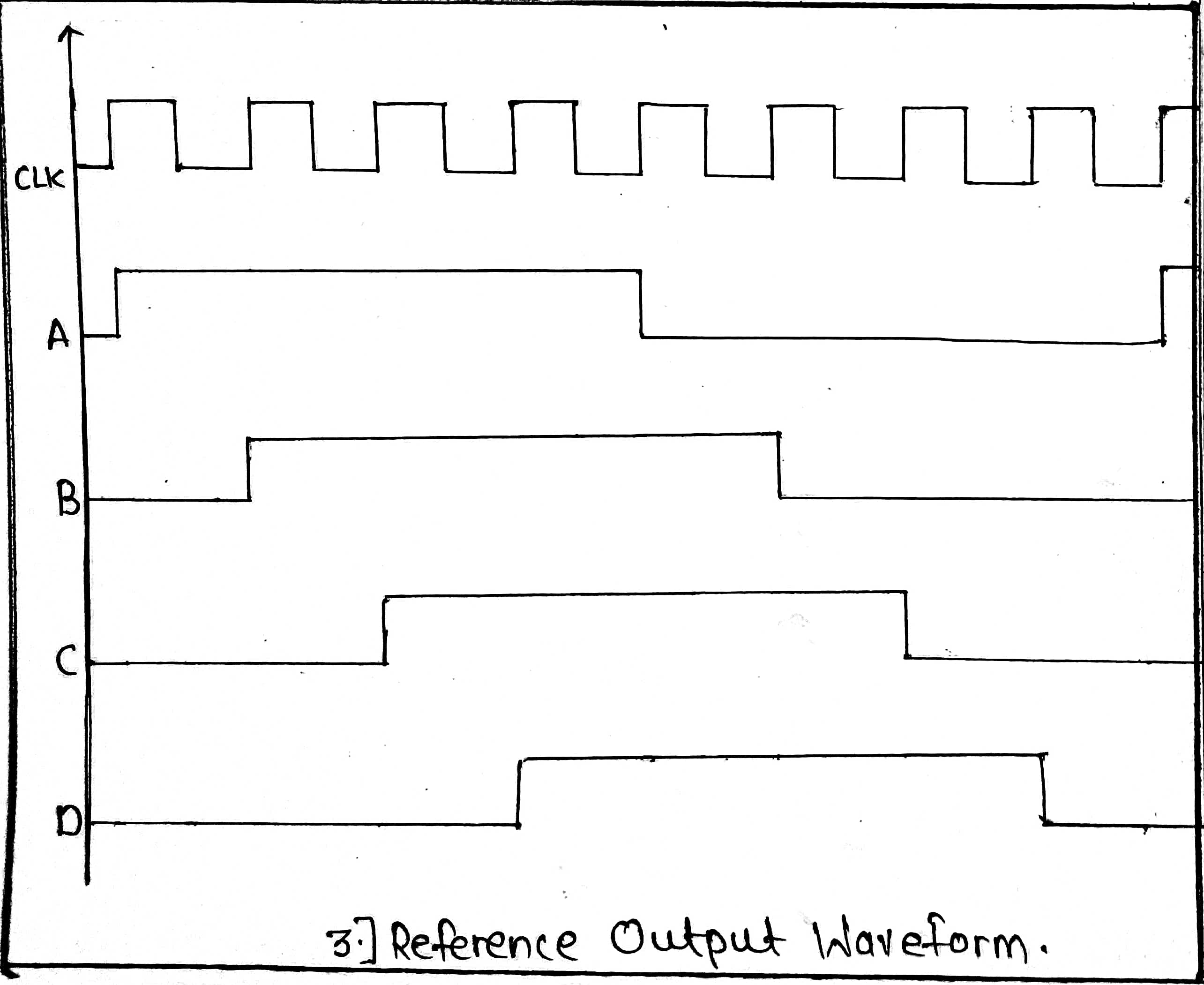
- REFERENCE CIRCUIT WAVEFORM
- REFERENCE CIRCUIT DIAGRAM
- IMPLEMENTATION
- REFERENCE
In this project, I am going to Design and Implement a 4-bit Johnson Counter with Ring Oscillator using Verilog HDL and SKY130nm PDK. Design will be implemented using Verilog Code using esim and Makerchip Software. Mixed Signal Circuits contain both analog and digital part of a circuit. In this design we have implemented Johnson counter using Verilog code and Ring oscillator using CMOS circuit. As this is a mixed signal circuit, we will have complete implementation from HDL code to schematic implementation and we can verify the output using Circuit Waveforms. This complete design and implementation is done using VLSI technology which has features such as high speed, low power, low cost, and small size.
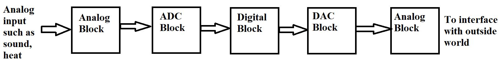
A Mixed signal integrated circuit is any integrated circuit that has both analog circuits and digital circuits on a single semiconductor die. A signal which continously varies with time is an Analog Signal. An analog signal can generally be represented as a function of time (f(t)).The signals which are basically generated from the nature are analog in nature. Similarly, signals which have discrete values are called Digital signals. These are represented in binary form (0 and 1). Mixed Signal Circuits contain both analog and digital signals. The below diagram shows basic block diagram of Mixed Signal Circuiits:
For more information: https://en.wikipedia.org/wiki/Mixed-signal_integrated_circuit
- VERILOG or Verify Logic is an Hardware Description Language commonly used in VLSI Design to create electronic circuits.
For more information: https://en.wikipedia.org/wiki/Verilog
- TL-Verilog or Transaction-Level Verilog is an extension to SystemVerilog that supports a new design methodology, called transaction-level design
For more information: https://www.redwoodeda.com/tl-verilog
esim is an open-source EDA tool used for circuit design and simulation. Using esim we can draw circuit using Kicad, generate netlist and simulate using Ngspice.
For more information: https://esim.fossee.in/home
The Download link for above eSim software is: https://esim.fossee.in/downloads
Makerchip provides free and instant access to the latest tools from your browser and from your desktop. This includes open-source tools and proprietary ones.
For more information: https://www.makerchip.com/
A Johnson counter is also known as a k‐bit switch‐tail ring counter with 2k decoding gates which provides output for 2k timing signals. A k‐bit ring counter circulates a single bit among the flip‐flops and can provide k distinguishable states. To double the number of states the shift register must be connected as a switch-tail ring counter. In a switch‐tail ring counter we connect the last flip flop to the input of first flip flop as shown in the reference diagrams. The register shifts its contents once to the right with every clock pulse, and at the same time, the complemented value of the E flip‐flop is transferred into the A flip‐ flop. Here, the last inverter’s output is connected to the first inverter’s input through a feedback path. It performs operations in a ring type fashion hence known as Ring oscillator. The number of inverter stages in this oscillator mainly depends on the frequency which we want to generate from this oscillator. Time period of ring oscillator(T)=2nTd where Td=Propagation delay of each inverter, Frequency of ring oscillator(f)=1/T and n=Number of inverters.
- Digital Block Diagram:

- Analog Block Diagram:

The Verilog code of Johnson Counter is as follows:
module Radha_Counter_Module( out,reset,clk);
input clk,reset;
output [3:0] out;
reg [3:0] q;
always @(posedge clk)
begin
if(reset)
q<=4'd0;
else
begin
q[3]<=q[2];
q[2]<=q[1];
q[1]<=q[0];
q[0]<=(~q[3]);
end
end
assign out=q;
endmodule
Initially we add the verilog file to Makerchip and run the code to get the expected waveform. Makerchip will itself create a TVL file and run the code.
Below is the .tvl code which will be generated by Makerchip.
\TLV_version 1d: tl-x.org \SV /* verilator lint_off UNUSED*/ /* verilator lint_off DECLFILENAME*/ /* verilator lint_off BLKSEQ*/ /* verilator lint_off WIDTH*/ /* verilator lint_off SELRANGE*/ /* verilator lint_off PINCONNECTEMPTY*/ /* verilator lint_off DEFPARAM*/ /* verilator lint_off IMPLICIT*/ /* verilator lint_off COMBDLY*/ /* verilator lint_off SYNCASYNCNET*/ /* verilator lint_off UNOPTFLAT / / verilator lint_off UNSIGNED*/ /* verilator lint_off CASEINCOMPLETE*/ /* verilator lint_off UNDRIVEN*/ /* verilator lint_off VARHIDDEN*/ /* verilator lint_off CASEX*/ /* verilator lint_off CASEOVERLAP*/ /* verilator lint_off PINMISSING*/ /* verilator lint_off BLKANDNBLK*/ /* verilator lint_off MULTIDRIVEN*/ /* verilator lint_off WIDTHCONCAT*/ /* verilator lint_off ASSIGNDLY*/ /* verilator lint_off MODDUP*/ /* verilator lint_off STMTDLY*/ /* verilator lint_off LITENDIAN*/ /* verilator lint_off INITIALDLY*/
//Your Verilog/System Verilog Code Starts Here: module Radha_Counter_Module( out,reset,clk); input clk,reset; output [3:0] out;
reg [3:0] q;
always @(posedge clk) begin
if(reset) q<=4'd0; else begin q[3]<=q[2]; q[2]<=q[1]; q[1]<=q[0]; q[0]<=(~q[3]); end end
assign out=q;
endmodule
//Top Module Code Starts here: module top(input logic clk, input logic reset, input logic [31:0] cyc_cnt, output logic passed, output logic failed); logic [3:0] out;//output //The $random() can be replaced if user wants to assign values Radha_Counter_Module Radha_Counter_Module(.clk(clk), .reset(reset), .out(out));
\TLV
//Add \TLV here if desired
\SV
endmodule
The below diagram shows output waveform on Makerchip window:

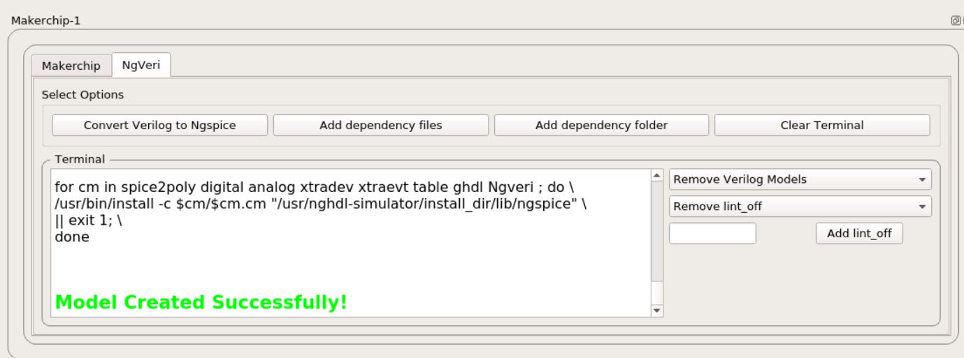
After debugging the verilog code we open the NgVeri tab and select Add Verilog to NgSpice converter to create the Mux model.
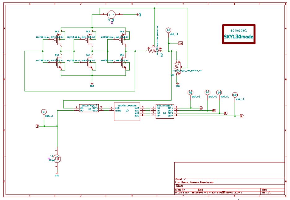
After successfully creating the model we create the schematic as shown in the below schematic diagram:
Create netlist and run kicad to ngspice converter. After giving the required timing parameters we will get a .cir.out file.
- /home/radhadk260501/esim-workspace/radha_johnson_counter/radha_johnson_counter.cir
.include "/usr/share/local/sky130_fd_pr/models/sky130_fd_pr__model__r+c.model.spice"
.lib "/usr/share/local/sky130_fd_pr/models/sky130.lib.spice" tt
.include "/usr/share/local/sky130_fd_pr/models/sky130_fd_pr__model__diode_pd2nw_11v0.model.spice"
.include "/usr/share/local/sky130_fd_pr/models/sky130_fd_pr__model__linear.model.spice"
.include "/usr/share/local/sky130_fd_pr/models/sky130_fd_pr__model__pnp.model.spice"
.include "/usr/share/local/sky130_fd_pr/models/sky130_fd_pr__model__diode_pw2nd_11v0.model.spice"
.include "/usr/share/local/sky130_fd_pr/models/sky130_fd_pr__model__inductors.model.spice"
-
u2 net-u2-pad1 net-u2-pad2 net-u2-pad3 net-u2-pad4 net-u2-pad5 net-u2-pad6 counter_module
-
u3 clk t net-u2-pad1 net-u2-pad2 adc_bridge_2
-
u4 net-u2-pad3 net-u2-pad4 net-u2-pad5 net-u2-pad6 a b c d dac_bridge_4
xsc7 net-sc1-pad2 clk net-sc1-pad3 sky130_fd_pr__res_generic_nd
xsc8 clk gnd net-sc1-pad3 sky130_fd_pr__res_generic_nd
v2 net-sc1-pad3 gnd dc 1.8
-
s c m o d e
-
u5 clk plot_v1
-
u6 a plot_v1
-
u7 b plot_v1
-
u8 c plot_v1
-
u9 d plot_v1
xsc2 net-sc1-pad1 net-sc1-pad2 gnd gnd sky130_fd_pr__nfet_01v8_lvt
xsc4 net-sc3-pad1 net-sc1-pad1 gnd gnd sky130_fd_pr__nfet_01v8_lvt
xsc6 net-sc1-pad2 net-sc3-pad1 gnd gnd sky130_fd_pr__nfet_01v8_lvt
xsc1 net-sc1-pad1 net-sc1-pad2 net-sc1-pad3 net-sc1-pad3 sky130_fd_pr__pfet_01v8_lvt
xsc3 net-sc3-pad1 net-sc1-pad1 net-sc1-pad3 net-sc1-pad3 sky130_fd_pr__pfet_01v8_lvt
xsc5 net-sc1-pad2 net-sc3-pad1 net-sc1-pad3 net-sc1-pad3 sky130_fd_pr__pfet_01v8_lvt
- u1 t plot_v1
v1 t gnd pulse(0 1.8 0.1 0.1 0.1 1 2)
a1 [net-u2-pad1 ] [net-u2-pad2 ] [net-u2-pad3 net-u2-pad4 net-u2-pad5 net-u2-pad6 ] u2
a2 [clk t ] [net-u2-pad1 net-u2-pad2 ] u3
a3 [net-u2-pad3 net-u2-pad4 net-u2-pad5 net-u2-pad6 ] [a b c d ] u4
- Schematic Name: counter_module, NgSpice Name: counter_module
.model u2 counter_module(rise_delay=1.0e-9 fall_delay=1.0e-9 input_load=1.0e-12 instance_id=1 )
- Schematic Name: adc_bridge_2, NgSpice Name: adc_bridge
.model u3 adc_bridge(in_low=1.0 in_high=2.0 rise_delay=1.0e-9 fall_delay=1.0e-9 )
- Schematic Name: dac_bridge_4, NgSpice Name: dac_bridge
.model u4 dac_bridge(out_low=0.0 out_high=5.0 out_undef=0.5 input_load=1.0e-12 t_rise=1.0e-9 t_fall=1.0e-9 )
.tran 5e-00 15e-00 0e-00
- Control Statements
.control
run
print allv > plot_data_v.txt
print alli > plot_data_i.txt
plot v(clk)
plot v(a)
plot v(b)
plot v(c)
plot v(d)
plot v(t)
.endc
.end
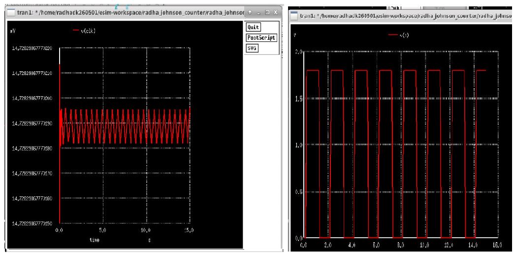
Now, we simulate the circuit using NgSpice to verify the logic of the circuit.
We will get waveforms as follows:
In this way we Design and implement a 4-bit Johnson Counter with Ring Oscillator.
[1] Stoev, I. I., Borodzhieva, A. N., & Mutkov, V. A. (2018). FPGA Implementation of Johnson Counters Applied in the Educational Process. 2018 IEEE 24th International Symposium for Design and Technology in Electronic Packaging (SIITME). doi:10.1109/siitme.2018.8599274
[2] V. Sikarwar, N. Yadav and S. Akashe, "Design and analysis of CMOS ring oscillator using 45 nm technology," 2013 3rd IEEE International Advance Computing Conference (IACC), Ghaziabad, 2013, pp. 1491- 149