- Abstract
- Reference Circuit Diagram
- Circuit Details
- Methodology
- Software Used
- Verilog Code
- MakerChip
- Waveforms
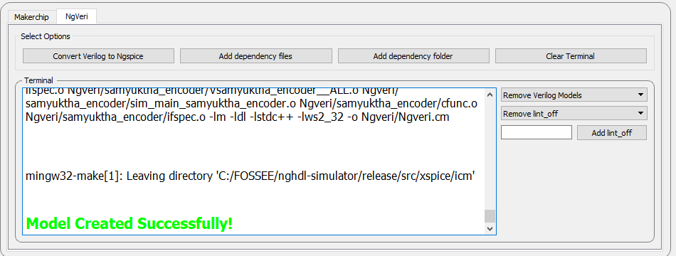
- Models created
- Schematics
- Netlist
- Output Waveform
- Author
- Acknowledgements
- Reference
Table of contents generated with markdown-toc
Capacitive sensors have more applications in the fields ranging from consumer electronics to automobiles, healthcare, and automation multiple design techniques are introduced for capacitive sensor readout circuits, that is also known as capacitance-to-digital converters (CDCs).T-capacitance to digital converter(CDC)moves the conversion process from the analog domain into the digital domain. It offers outstanding flexibility with respect to power consumption, resolution and speed.

The sensor capacitance is the load capacitance of a voltage-to-time converter (VTC) circuit based on current starved inverters. The VTC circuit used has improved sensitivity, linearity and dynamic range. The time delay provided by the VTC circuit is buffered providing a time pulse proportional to the sensor capacitance (C s ). Thus, the VTC circuit becomes a capacitance-to-time converter (CTC) circuit. The time pulse is then digitized using a time-to-digital converter (TDC) circuit providing an output digital code proportional to the sensor capacitance. T-CDC system is a time-based ADC, but with the sensor capacitance as the load capacitance of the used VTC circuit and the input voltages of the current starved inverters in the VTC circuit are fixed and used for biasing.
Verilog code for 2 input nand gate, 3 input nand gate, Multiplexer and priority encoder is created and simulated using MakerChip. The Code is dumped in Ngveri and model is created. Schematics is drawn on eSim. Generating Netlist for the mixed signal circuit. Kicad to Ngspice conversion is done by adding simulation parameters for the circuit. Simulation is done.
eSim:
It is an Open Source EDA developed by FOSSEE, IIT Bombay. It is used for electronic circuit simulation. It is made by the combination of two software namely NgSpice and KiCAD. For more details refer: https://esim.fossee.in/home
NgSpice:
It is an Open Source Software for Spice Simulations. For more details refer: http://ngspice.sourceforge.net/docs.html
Makerchip:
It is an Online Web Browser IDE for Verilog/System-verilog/TL-Verilog Simulation. Refer https://www.makerchip.com/
Verilator:
It is a tool which converts Verilog code to C++ objects. Refer: https://www.veripool.org/verilator/
Verilog code for 2 input nand gate:
Verilog code for 3 input nand gate

Verilog Code for 2:1 Multiplexer
Verilog code for priority encoder

Code for 3 input nand gate:
\TLV_version 1d: tl-x.org \SV /* verilator lint_off UNUSED*/ /* verilator lint_off DECLFILENAME*/ /* verilator lint_off BLKSEQ*/ /* verilator lint_off WIDTH*/ /* verilator lint_off SELRANGE*/ /* verilator lint_off PINCONNECTEMPTY*/ /* verilator lint_off DEFPARAM*/ /* verilator lint_off IMPLICIT*/ /* verilator lint_off COMBDLY*/ /* verilator lint_off SYNCASYNCNET*/ /* verilator lint_off UNOPTFLAT / / verilator lint_off UNSIGNED*/ /* verilator lint_off CASEINCOMPLETE*/ /* verilator lint_off UNDRIVEN*/ /* verilator lint_off VARHIDDEN*/ /* verilator lint_off CASEX*/ /* verilator lint_off CASEOVERLAP*/ /* verilator lint_off PINMISSING*/ /* verilator lint_off LATCH*/ /* verilator lint_off BLKANDNBLK*/ /* verilator lint_off MULTIDRIVEN*/ /* verilator lint_off NULLPORT*/ /* verilator lint_off EOFNEWLINE*/ /* verilator lint_off WIDTHCONCAT*/ /* verilator lint_off ASSIGNDLY*/ /* verilator lint_off MODDUP*/ /* verilator lint_off STMTDLY*/ /* verilator lint_off LITENDIAN*/ /* verilator lint_off INITIALDLY*/ /* verilator lint_off */
//Your Verilog/System Verilog Code Starts Here: module sam_nand3(a,b,c,d); input a,b,c; output d; nand n1(d,a,b,c); endmodule
//Top Module Code Starts here: module top(input logic clk, input logic reset, input logic [31:0] cyc_cnt, output logic passed, output logic failed); logic a;//input logic b;//input logic c;//input logic d;//output //The $random() can be replaced if user wants to assign values assign a = $random(); assign b = $random(); assign c = $random(); sam_nand3 sam_nand3(.a(a), .b(b), .c(c), .d(d));
\TLV
//Add \TLV here if desired
\SV
endmodule
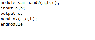
Code for 2 input nand gate :
\TLV_version 1d: tl-x.org \SV /* verilator lint_off UNUSED*/ /* verilator lint_off DECLFILENAME*/ /* verilator lint_off BLKSEQ*/ /* verilator lint_off WIDTH*/ /* verilator lint_off SELRANGE*/ /* verilator lint_off PINCONNECTEMPTY*/ /* verilator lint_off DEFPARAM*/ /* verilator lint_off IMPLICIT*/ /* verilator lint_off COMBDLY*/ /* verilator lint_off SYNCASYNCNET*/ /* verilator lint_off UNOPTFLAT / / verilator lint_off UNSIGNED*/ /* verilator lint_off CASEINCOMPLETE*/ /* verilator lint_off UNDRIVEN*/ /* verilator lint_off VARHIDDEN*/ /* verilator lint_off CASEX*/ /* verilator lint_off CASEOVERLAP*/ /* verilator lint_off PINMISSING*/ /* verilator lint_off LATCH*/ /* verilator lint_off BLKANDNBLK*/ /* verilator lint_off MULTIDRIVEN*/ /* verilator lint_off NULLPORT*/ /* verilator lint_off EOFNEWLINE*/ /* verilator lint_off WIDTHCONCAT*/ /* verilator lint_off ASSIGNDLY*/ /* verilator lint_off MODDUP*/ /* verilator lint_off STMTDLY*/ /* verilator lint_off LITENDIAN*/ /* verilator lint_off INITIALDLY*/ /* verilator lint_off */
//Your Verilog/System Verilog Code Starts Here: module sam_nand2(a,b,c); input a,b; output c; nand n2(c,a,b); endmodule
//Top Module Code Starts here: module top(input logic clk, input logic reset, input logic [31:0] cyc_cnt, output logic passed, output logic failed); logic a;//input logic b;//input logic c;//output //The $random() can be replaced if user wants to assign values assign a = $random(); assign b = $random(); sam_nand2 sam_nand2(.a(a), .b(b), .c(c));
\TLV
//Add \TLV here if desired
\SV
endmodule
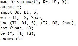
Code for 2:1 Multiplexer:
\TLV_version 1d: tl-x.org \SV /* verilator lint_off UNUSED*/ /* verilator lint_off DECLFILENAME*/ /* verilator lint_off BLKSEQ*/ /* verilator lint_off WIDTH*/ /* verilator lint_off SELRANGE*/ /* verilator lint_off PINCONNECTEMPTY*/ /* verilator lint_off DEFPARAM*/ /* verilator lint_off IMPLICIT*/ /* verilator lint_off COMBDLY*/ /* verilator lint_off SYNCASYNCNET*/ /* verilator lint_off UNOPTFLAT / / verilator lint_off UNSIGNED*/ /* verilator lint_off CASEINCOMPLETE*/ /* verilator lint_off UNDRIVEN*/ /* verilator lint_off VARHIDDEN*/ /* verilator lint_off CASEX*/ /* verilator lint_off CASEOVERLAP*/ /* verilator lint_off PINMISSING*/ /* verilator lint_off LATCH*/ /* verilator lint_off BLKANDNBLK*/ /* verilator lint_off MULTIDRIVEN*/ /* verilator lint_off NULLPORT*/ /* verilator lint_off EOFNEWLINE*/ /* verilator lint_off WIDTHCONCAT*/ /* verilator lint_off ASSIGNDLY*/ /* verilator lint_off MODDUP*/ /* verilator lint_off STMTDLY*/ /* verilator lint_off LITENDIAN*/ /* verilator lint_off INITIALDLY*/ /* verilator lint_off */
//Your Verilog/System Verilog Code Starts Here: module sam_mux(Y, D0, D1, S); output Y; input D0, D1, S; wire T1, T2, Sbar; and (T1, D1, S), (T2, D0, Sbar); not (Sbar, S); or (Y, T1, T2); endmodule
//Top Module Code Starts here: module top(input logic clk, input logic reset, input logic [31:0] cyc_cnt, output logic passed, output logic failed); logic Y;//output logic D0;//input logic D1;//input logic S;//input //The $random() can be replaced if user wants to assign values assign D0 = $random(); assign D1 = $random(); assign S = $random(); sam_mux sam_mux(.Y(Y), .D0(D0), .D1(D1), .S(S));
\TLV
//Add \TLV here if desired
\SV
endmodule
Code for priority encoder :
\TLV_version 1d: tl-x.org \SV /* verilator lint_off UNUSED*/ /* verilator lint_off DECLFILENAME*/ /* verilator lint_off BLKSEQ*/ /* verilator lint_off WIDTH*/ /* verilator lint_off SELRANGE*/ /* verilator lint_off PINCONNECTEMPTY*/ /* verilator lint_off DEFPARAM*/ /* verilator lint_off IMPLICIT*/ /* verilator lint_off COMBDLY*/ /* verilator lint_off SYNCASYNCNET*/ /* verilator lint_off UNOPTFLAT / / verilator lint_off UNSIGNED*/ /* verilator lint_off CASEINCOMPLETE*/ /* verilator lint_off UNDRIVEN*/ /* verilator lint_off VARHIDDEN*/ /* verilator lint_off CASEX*/ /* verilator lint_off CASEOVERLAP*/ /* verilator lint_off PINMISSING*/ /* verilator lint_off LATCH*/ /* verilator lint_off BLKANDNBLK*/ /* verilator lint_off MULTIDRIVEN*/ /* verilator lint_off NULLPORT*/ /* verilator lint_off EOFNEWLINE*/ /* verilator lint_off WIDTHCONCAT*/ /* verilator lint_off ASSIGNDLY*/ /* verilator lint_off MODDUP*/ /* verilator lint_off STMTDLY*/ /* verilator lint_off LITENDIAN*/ /* verilator lint_off INITIALDLY*/ /* verilator lint_off */
//Your Verilog/System Verilog Code Starts Here: module sam_mux(Y, D0, D1, S); output Y; input D0, D1, S; wire T1, T2, Sbar; and (T1, D1, S), (T2, D0, Sbar); not (Sbar, S); or (Y, T1, T2); endmodule
//Top Module Code Starts here: module top(input logic clk, input logic reset, input logic [31:0] cyc_cnt, output logic passed, output logic failed); logic Y;//output logic D0;//input logic D1;//input logic S;//input //The $random() can be replaced if user wants to assign values assign D0 = $random(); assign D1 = $random(); assign S = $random(); sam_mux sam_mux(.Y(Y), .D0(D0), .D1(D1), .S(S));
\TLV
//Add \TLV here if desired
\SV
endmodule
Waveform for 2 input gate gate:

Waveform for 3 input nand gate :

Waveform for 2:1 Mux

Waveform for priority encoder

Model created for 2 input nand gate:
Like wise models were created for 3 input nand gate, priority encoder and 2:1 Mux using Ngveri

Charge pumping circuit with Voltage to Time converter part

Time to Digital Converter part


Samyuktha Shrruthi K R
Final Year B.E. ECE
Easwari Engineering College
Mail : samyukthashrruthi@gmail.com
- Kunal Ghosh (Co-Founder, VLSI System Design Pvt. Ltd.)
- FOSSEE, IIT Bombay
- Steve Hoover (Founder, Redwood EDA)
- Sumanto Kar (eSim Team, FOSSEE, IIT Bombay)
- A. Fouad, Y. Ismail and H. Mostafa, "Design of a time-based capacitance-to-digital converter using current starved inverters," 2017 29th International Conference on Microelectronics (ICM), 2017, pp. 1-4, doi: 10.1109/ICM.2017.8268882.