This repository shows the design of conventional PLL using Synopsys Custom Compiler at 28nm CMOS technology.
The prime focus of this paper to design a conventional PLL with low power consumption and low area. The design is to be implemented in 28nm CMOS technology. Usulally as technology scale down a PLL with wide tuning range, low jitter, and PLL operating at high frequencies are preferred.
A phase-locked loop or PLL is a closed loop feedback circuit comprises of four main blocks phase frequency detector (PFD), charge pump (CP), low pass filter (LPF) and voltage-controlled oscillator (VCO) PLL as shown in Fig.1. These blocks are connected to form a closed loop feedback network so as to synchronize the output with the input in both phase and frequency. And this loop continues to run until PLL locked condition is achieved i.e., either zero or constant phase difference between the reference input and the feedback pulse from the output of PLL. PLL is castoff as on chip clock generator, frequency synthesizer and clock and data recovery system in radio, computers and telecommunication system. In general, as technology scale down a PLL with wide tuning range, low jitter, and PLL operating at high frequencies are preferred.
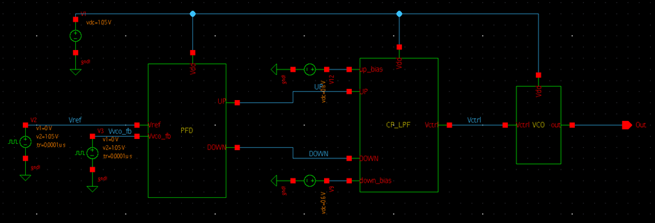
In Fig. 1, to feedback output from VCO to PFD one extra block is needed i.e., frequency divider so instead an extra pulse voltage source is placed.
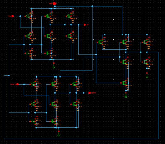
The concept behind PFD is it compare the two-input signal and produces error signal proportional to the difference between the input signals so for PLL it is used as error detecting block. PFD uses two D-FF's whose input is kept always at high potential, and the reference signal is provided at the clock input of one the D-FF i.e., CLKREF and output of VCO is feed-back to clock input of another D-FF i.e., CLKFB. An AND gate is provided at the output of both D-FFs to generate a reset signal and set the output of both the D-FFs to zero whenever both the signal QA or UP and QB or DOWN is high.
A charge pump is a bipolar switch that is controlled by the three states of the PFD. Conventional charge pump has two symmetrical current sources and two transistors that acts as switch. It generates both the polarity of current pulses into LPF. LPF is used in PLL to get rid of the high frequency components in the output of the PFD. It also removes the high frequency noise.
VCO is the most important block in PLL. It produces high frequency output signal in phase with reference input signal to PLL. In an ideal VCO, there is a linear relationship between output frequency and control voltage.
In reference to circuit design D-FF cast-off in PFD are using TSPC based logic scheme since it operates at high speed and consumes low power and area [2]. Conventional CP and three stage ring VCO are been implemented as shown in Fig. 2(b) & (c). Additional two transistor in VCO are used works as resistor to limit current to circuit and capacitors are used for smoothing the output waveform and remove spikes from output.
When the UP signal is generated (high) as shown in Fig. 3, this signifies that the reference signal is leading the VCO output so to match the reference signal and feedback signal VCO input must be tuned such that it generates a high-frequency output signal. This process continues till both the signal matches and PLL enters into lock condition. Similarly, when the DOWN signal is generated (high) this signifies that VCO output leads the reference signal so VCO must be tuned such that it generates a low output frequency till it matches with reference signal.


As shown in Fig. 3(a) when reference signal leads the feedback signal UP signal is generated (logic 1) and current through charge-pump start to increase and vive-versa when reference signal lags feedback signal as shown in Fig. (b). The voltage appear acrosss LPF which work as input voltage to VCO also known as control voltage which is propotional to the error pulse width.
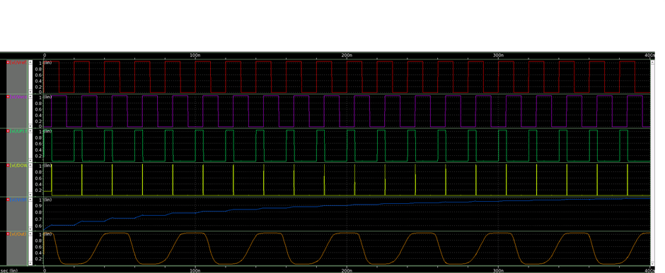
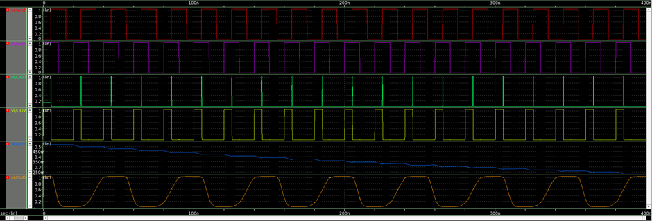
Fig. 3. (a)When reference signal leads feedback signal (b) When reference signal lags feedback signal
- Shubham Tomar, M.Tech(VLSI and Embedded Systems), Dhirubhai Ambani Institue of Information and Communication Technology, Gujarat.
- Kunal Ghosh, Co-founder, VSD Corp. Pvt. Ltd. - kunalpghosh@gmail.com
- Cloud Based Analog IC Design Hackathon, IIT Hyderabad
- Synopsys India
[1] Razavi, B. (2005). Design of analog CMOS integrated circuits.
[2] Kailuke, A. C., Agrawal, P., & Kshirsagar, R. V. (2014, January). Design of phase frequency detector and charge pump for low voltage high frequency PLL. In 2014 International Conference on Electronic Systems, Signal Processing and Computing Technologies (pp. 74-78). IEEE.
[3] Goyal, B., Suman, S., & Ghosh, P. K. (2016, March). Design of charge pump PLL using improved performance ring VCO. In 2016 International Conference on Electrical, Electronics, and Optimization Techniques (ICEEOT) (pp. 3254-3258). IEEE.
[4] Ratan, R. (2014). Design of a phase locked loop based clocking circuit for high speed serial link applications.