This repository contains information about a 3 bit up counter with synchronus buffered reset implemented on esim using SKY130 PDK.
- Abstract
- Reference Circuit Diagram
- Reference Waveform
- Circuit Details
- Software Used
- Circuit Schematic in eSim
- Verilog Code
- Makerchip
- Makerchip plots
- Netlist
- NgSpice Plots
- GAW Plots
- Steps to run generate NgVeri Model
- Steps to run this project
- Author
- Acknowledgements
- References
Counters are digital circuits widely used in various applications like counting, frequency divisions, memory increment in the registers, etc. In this project, the design of a 3-bit up counter with synchronus reset is described where the reset is buffered for better performance.
The refrence circuit diagram along with the abstraction is depicted in Fig 1.

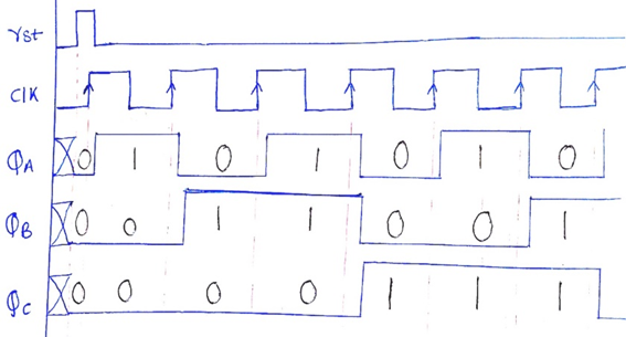
The refrence waveform for depiction of wokring of counter is attached below in Fig 2. (although the refrence waveform showing asynchronus reset, actual design is implemented with synchronus reset)
The up counter is designed using back to back connected CMOS 2-Tx based inverter based buffer made on sky 130nm technology to buffer the reset signal hence to avoid any possible synchronization errors. Then the reset signal is passed to the reset input of the counter block for furthur operation.
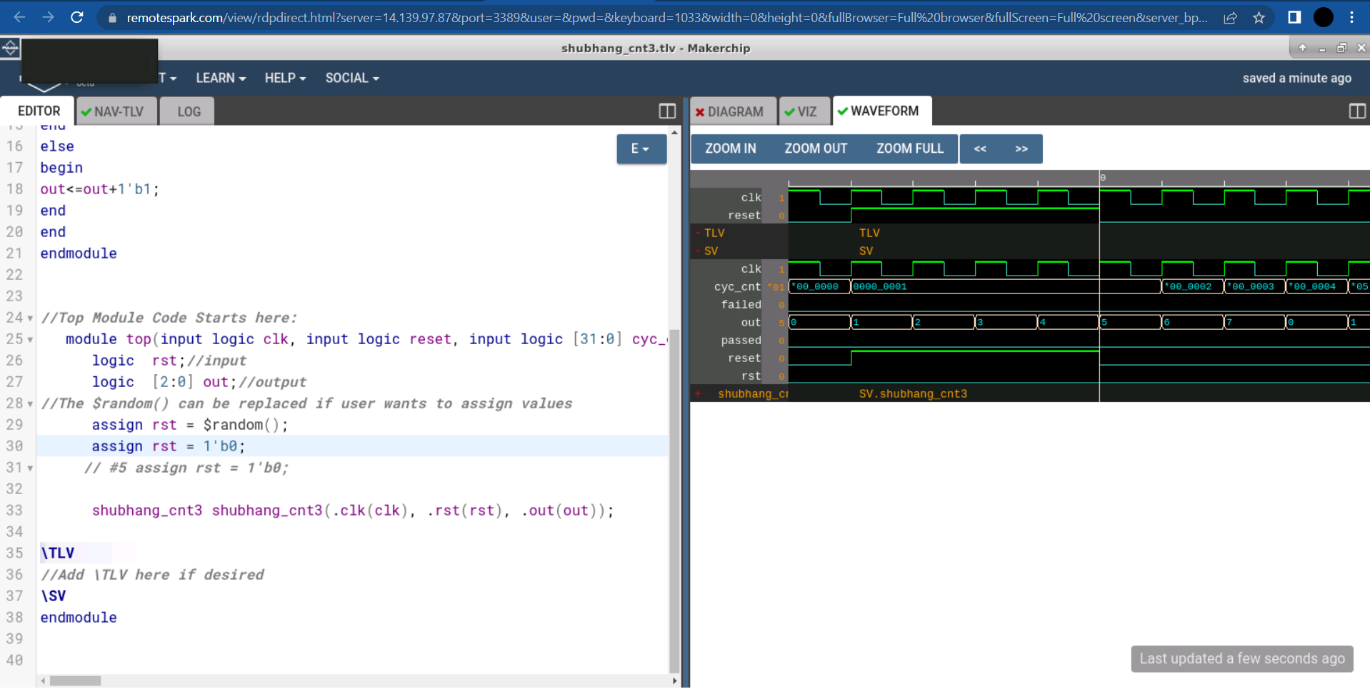
The counter is made on Verilog and verified using makerchip IDE and is a fully synthesizable block.
To interface the analog and digital signals the dac and adc bridges from esim hybrid are used (The default ouput values of dac are set to be 2V for high and 0V for low despite supply being 3V to differentiate and make the understanding of output easier).
- eSim is an Open Source EDA developed by FOSSEE, IIT Bombay. It is used for electronic circuit simulation. It is made by the combination of two software namely NgSpice and KiCAD.
For more details refer:
https://esim.fossee.in/home
- ng spice is an Open Source Software for Spice Simulations. For more details refer:
http://ngspice.sourceforge.net/docs.html
- Makerchip is an Online Web Browser IDE for Verilog/System-verilog/TL-Verilog Simulation. Refer
https://www.makerchip.com/
- Verilator is a tool which converts Verilog code to C++ objects. Refer: https://www.veripool.org/verilator/

Fig 3: Circuit Schematic
The verilog code for the used counter is given below:
module shubhang_cnt3(clk,rst,out);
input clk,rst;
output reg [2:0]out;
always @(posedge clk)
begin
if (rst)
begin
out<=3'b0;
end
else
begin
out<=out+1'b1;
end
end
endmodule
\TLV_version 1d: tl-x.org
\SV
/* verilator lint_off UNUSED*/  /* verilator lint_off DECLFILENAME*/  /* verilator lint_off BLKSEQ*/  /* verilator lint_off WIDTH*/  /* verilator lint_off SELRANGE*/  /* verilator lint_off PINCONNECTEMPTY*/  /* verilator lint_off DEFPARAM*/  /* verilator lint_off IMPLICIT*/  /* verilator lint_off COMBDLY*/  /* verilator lint_off SYNCASYNCNET*/  /* verilator lint_off UNOPTFLAT */  /* verilator lint_off UNSIGNED*/  /* verilator lint_off CASEINCOMPLETE*/  /* verilator lint_off UNDRIVEN*/  /* verilator lint_off VARHIDDEN*/  /* verilator lint_off CASEX*/  /* verilator lint_off CASEOVERLAP*/  /* verilator lint_off PINMISSING*/  /* verilator lint_off LATCH*/  /* verilator lint_off BLKANDNBLK*/  /* verilator lint_off MULTIDRIVEN*/  /* verilator lint_off NULLPORT*/  /* verilator lint_off EOFNEWLINE*/  /* verilator lint_off WIDTHCONCAT*/  /* verilator lint_off ASSIGNDLY*/  /* verilator lint_off MODDUP*/  /* verilator lint_off STMTDLY*/  /* verilator lint_off LITENDIAN*/  /* verilator lint_off INITIALDLY*/  /* verilator lint_off */

//Your Verilog/System Verilog Code Starts Here:
module shubhang_cnt3(clk,rst,out);
input clk,rst;
output reg [2:0]out;

always @(posedge clk)
begin
if (rst)
begin
out<=3'b0;
end
else
begin
out<=out+1'b1;
end
end
endmodule


//Top Module Code Starts here:
	module top(input logic clk, input logic reset, input logic [31:0] cyc_cnt, output logic passed, output logic failed);
		logic  rst;//input
		logic  [2:0] out;//output
//The $random() can be replaced if user wants to assign values
		assign rst = $random();
		shubhang_cnt3 shubhang_cnt3(.clk(clk), .rst(rst), .out(out));

\TLV
//Add \TLV here if desired
\SV
endmodule
Fig 4 Depicts the Makerchip Plots.
* /home/2019uee0117/esim-workspace/counter/counter.cir

.lib "/usr/share/local/sky130_fd_pr/models/sky130.lib.spice" tt
.include "/usr/share/local/sky130_fd_pr/models/sky130_fd_pr__model__diode_pd2nw_11v0.model.spice"
.include "/usr/share/local/sky130_fd_pr/models/sky130_fd_pr__model__pnp.model.spice"
.include "/usr/share/local/sky130_fd_pr/models/sky130_fd_pr__model__diode_pw2nd_11v0.model.spice"
.include "/usr/share/local/sky130_fd_pr/models/sky130_fd_pr__model__r+c.model.spice"
.include "/usr/share/local/sky130_fd_pr/models/sky130_fd_pr__model__inductors.model.spice"
.include "/usr/share/local/sky130_fd_pr/models/sky130_fd_pr__model__linear.model.spice"
* u1  net-_u1-pad1_ net-_u1-pad2_ net-_u1-pad3_ net-_u1-pad4_ net-_u1-pad5_ shubhang_cnt3
xsc4 net-_sc3-pad1_ net-_sc1-pad1_ gnd gnd sky130_fd_pr__nfet_01v8
xsc3 net-_sc3-pad1_ net-_sc1-pad1_ dc dc sky130_fd_pr__pfet_01v8
xsc1 net-_sc1-pad1_ rst dc dc sky130_fd_pr__pfet_01v8
xsc2 net-_sc1-pad1_ rst gnd gnd sky130_fd_pr__nfet_01v8
* u2  net-_sc3-pad1_ net-_u1-pad2_ adc_bridge_1
v3  clk gnd pulse(0 3 0 1u 1u 0.1m 0.2m)
v1  rst gnd pulse(0 3 0 1u 1u 1m 2m)
* u3  clk net-_u1-pad1_ adc_bridge_1
* u4  net-_u1-pad3_ net-_u1-pad4_ net-_u1-pad5_ a b c dac_bridge_3
v2  gnd  dc 3
* u5  a plot_v1
* u7  b plot_v1
* u6  c plot_v1
* s c m o d e
* u9  clk plot_v1
* u8  rst plot_v1
a1 [net-_u1-pad1_ ] [net-_u1-pad2_ ] [net-_u1-pad3_ net-_u1-pad4_ net-_u1-pad5_ ] u1
a2 [net-_sc3-pad1_ ] [net-_u1-pad2_ ] u2
a3 [clk ] [net-_u1-pad1_ ] u3
a4 [net-_u1-pad3_ net-_u1-pad4_ net-_u1-pad5_ ] [a b c ] u4
* Schematic Name:                             shubhang_cnt3, NgSpice Name: shubhang_cnt3
.model u1 shubhang_cnt3(rise_delay=1.0e-9 fall_delay=1.0e-9 input_load=1.0e-12 instance_id=1 )
* Schematic Name:                             adc_bridge_1, NgSpice Name: adc_bridge
.model u2 adc_bridge(in_low=1.0 in_high=2.0 rise_delay=1.0e-9 fall_delay=1.0e-9 )
* Schematic Name:                             adc_bridge_1, NgSpice Name: adc_bridge
.model u3 adc_bridge(in_low=1.0 in_high=2.0 rise_delay=1.0e-9 fall_delay=1.0e-9 )
* Schematic Name:                             dac_bridge_3, NgSpice Name: dac_bridge
.model u4 dac_bridge(out_low=0 out_high=2 out_undef=0.5 input_load=1.0e-12 t_rise=1.0e-9 t_fall=1.0e-9 )
.tran 1e-03 10e-03 0e-00

* Control Statements
.control
run
print allv > plot_data_v.txt
print alli > plot_data_i.txt
plot v(a)
plot v(b)
plot v(c)
plot v(clk)
plot v(rst)
.endc
.end
Transient Simulation was done, the ouput file generated for the test is mentioned below:

Fig 5: vc (LSB of counter output)
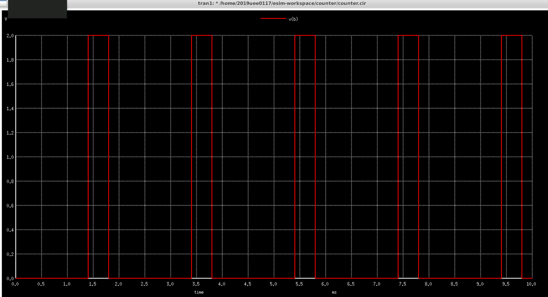
Fig 6: vb (middle bit of counter output)

Fig 7: va (MSB of counter output)

Fig 8: clock signal

Fig 9: reset (given perioidcally to show its working more clearly)
Fig 10 Represents GAW plot.

- Open eSim
- Run NgVeri-Makerchip
- Add top level verilog file in Makerchip Tab
- Click on NgVeri tab
- Add dependency files
- Click on Run Verilog to NgSpice Converter
- Debug if any errors
- Model created successfully
To run the project in eSim:
- Run eSim (On Virtual machine it needs to be evoked from the terminal)
- Load the project
- Open eeSchema
Shubhang Srivastava
Student
IC ResQ Lab
Dept of Electrical engineering
Indian Institute of Technology Jammu 181221
I would like to give my sincere thanks to undermentioned Organization/Persons for their invaluable guidance and software support which enabled me to participate and learn a lot from this Hackathon:
- Indian Institute of Technology Bombay (http://iitb.ac.in/)
- Google (https://www.google.co.in/)
- FOSSEE (https://fossee.in/)
- Spoken Tutorials (https://spoken-tutorial.org/)
- VSD (https://www.vlsisystemdesign.com)
- Chips to Startup Gov of India (https://www.c2s.gov.in/)
- Sumanto Kar (Sr Project Technical Assistant at IITB)
[1] Maekawa, Tomoaki & Amakawa, Shuhei & Ishihara, Noboru & Masu, Kazuya. (2009). Design of CMOS inverter-based output buffers adapting the Cherry-Hooper broadbanding technique. 511 - 514. 10.1109/ECCTD.2009.5275025.
[2] Mariyamol, p.p & Aswathy, N.. (2016). CMOS Buffer Design Approach for Low Power and Lower Delay SRAM Design. Procedia Technology. 25. 481-488. 10.1016/j.protcy.2016.08.135.
[3] Thomas L. Floyd “Digital Fundamentals”, 11th ed global edition, pp. 507-527