- Introduction
- Reference Circuit Diagram
- Circuit Details
- Resolution of ADC
- Designing Steps
- Open Source Tools Used
- Verilog Code
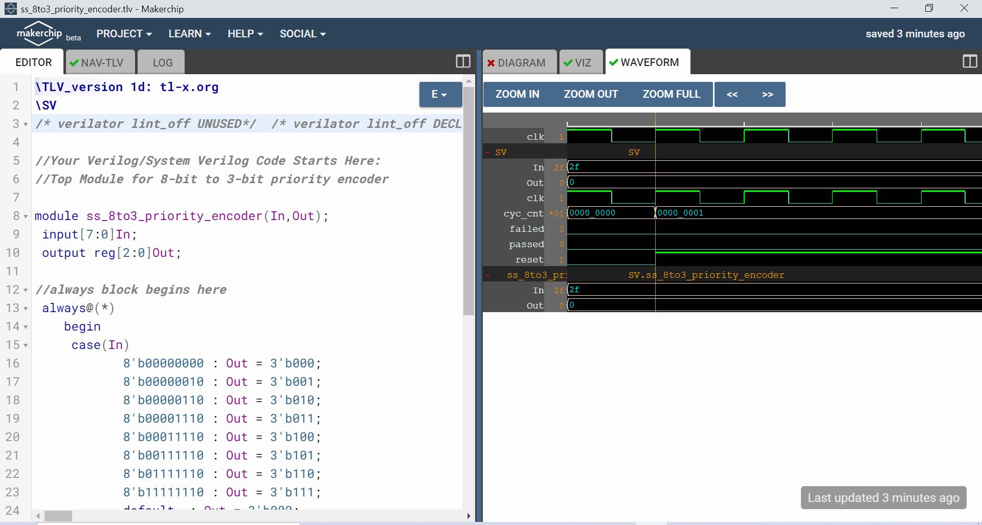
- Makerchip
- Model Creating for Priority Encoder using NgVeri
- Schematics
- Netlist
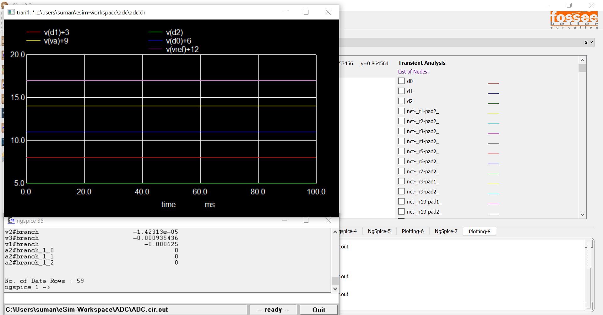
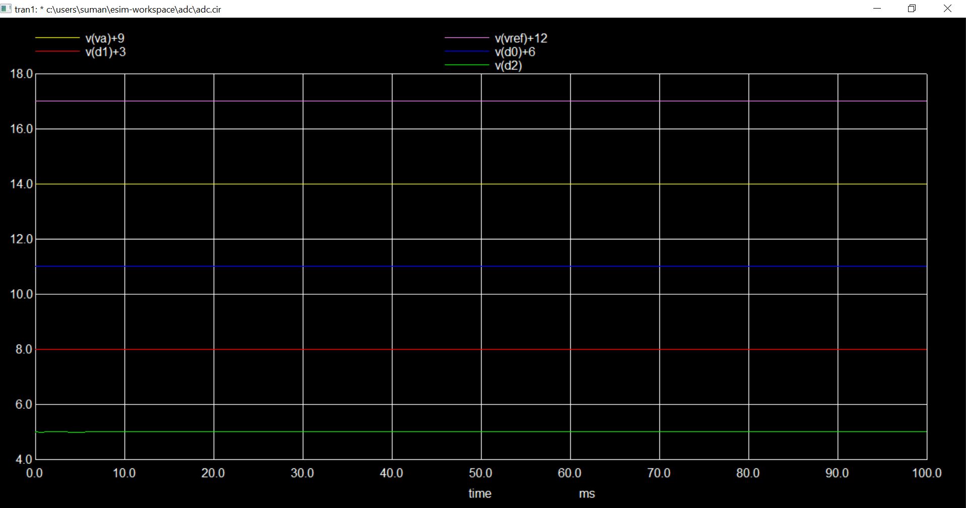
- Output Waveforms
- Author
- Acknowledgements
- References
This paper is about designing of a 3-bit Flash Type Analog-to-Digital Converter (ADC). Comparators and voltage divider circuits are used which are to be modelled using Ngspice and Priority encoder is designed using Verilog HDL. This is an example of mixed-signal electronic circuit simulation. Here, I have used eSim open-source EDA tool for the circuit design and simulation.
Given attached is the circuit diagram for 3-bit Flash Type ADC.
Fig. 1: 3-bit Flash Type ADC
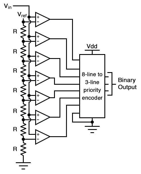
Flash analog to digital converter is the fastest type of ADC among all the other ADCs. It is also known as a parallel analog to digital converter. It comprises high-speed comparators, resistive voltage divider circuits along with a priority encoder. Each stage of the divider is connected to one input of a comparator and the input signal is applied in parallel to the other input of all the comparators. The outputs of the comparators are connected to some combinational logic which detects which of the comparator outputs are high and which are low, and provides the appropriately coded digital output.
The ADC resolution is defined as the smallest incremental voltage that can be recognized and thus causes a change in the digital output. It is expressed as the number of bits output by the ADC. In our design, we are keeping Vref as 5V, hence resolution of proposed ADC design is given by the formula :
𝑅𝑒𝑠𝑜𝑙𝑢𝑡𝑖𝑜𝑛 = (𝑅𝑒𝑓𝑒𝑟𝑒𝑛𝑐𝑒 𝑉𝑜𝑙𝑡𝑎𝑔𝑒)/2^n = 5/2^3 = 5/8 = 0.625V
Where, n is the number of output binary bits.
• Step 1 : Writing Verilog code for 8:3 Priority Encoder & simulating on Makerchip. File name and top module of Verilog Code should be same.
• Step 2 : Model creation on NgVeri and simulating using Makerchip.
• Step 3 : Schematics creation using Eeschema.
• Step 4 : Annotating schematic and Running Electrical Rule Check (ERC) and then Creating Netlist.
• Step 5 : Setting simulation instance parameters on KicadToNgspice Converter.Also adding path to subcircuits before converting to Ngspice.
• Step 6: Simulation & Verification of results.
eSim
It is an Open Source EDA developed by FOSSEE, IIT Bombay. It is used for electronic circuit simulation. It is made by the combination of two software namely NgSpice and KiCAD. For more details refer:
NgSpice
It is an Open Source Software for Spice Simulations. For more details refer:
http://ngspice.sourceforge.net/docs.html
Makerchip
It is an Online Web Browser IDE for Verilog/System-verilog/TL-Verilog Simulation. For more details refer:
Verilator
It is a tool which converts Verilog code to C++ objects. For more details refer:
https://www.veripool.org/verilator/
      `timescale 1ns / 1ps
      //////////////////////////////////////////////////////////////////////////////////
      // Mixed Signal Design Hacakthon
      //
      // (Organized by FOSSEE IIT Bombay, VSD Corp. Pvt. Ltd., Redwood EDA)
      //
      // Design Name: 		8:3 Encoder
      // Designer :	 	Sumanyu Singh
      // Module Name:    	ss_8to3_priority_encoder
      //
      //////////////////////////////////////////////////////////////////////////////////

     module ss_8to3_priority_encoder(In,Out);
        input[7:0]In;
        output reg[2:0]Out;

        //always block begins here
     always@(*)
       begin
          case(In)
            8'b00000000 : Out = 3'b000;
            8'b00000010 : Out = 3'b001;
            8'b00000110 : Out = 3'b010;
            8'b00001110 : Out = 3'b011;
            8'b00011110 : Out = 3'b100;
            8'b00111110 : Out = 3'b101;
            8'b01111110 : Out = 3'b110;
            8'b11111110 : Out = 3'b111;
             default  : Out = 3'b000;
        endcase
       end

      endmodule
     \TLV_version 1d: tl-x.org
     \SV
     /* verilator lint_off UNUSED*/  /* verilator lint_off DECLFILENAME*/  /* verilator lint_off BLKSEQ*/  /* verilator lint_off WIDTH*/  /* verilator lint_off SELRANGE*/          /* verilator lint_off PINCONNECTEMPTY*/  /* verilator lint_off DEFPARAM*/  /* verilator lint_off IMPLICIT*/  /* verilator lint_off COMBDLY*/  /* verilator lint_off             SYNCASYNCNET*/  /* verilator lint_off UNOPTFLAT */  /* verilator lint_off UNSIGNED*/  /* verilator lint_off CASEINCOMPLETE*/  /* verilator lint_off UNDRIVEN*/  /*             verilator lint_off VARHIDDEN*/  /* verilator lint_off CASEX*/  /* verilator lint_off CASEOVERLAP*/  /* verilator lint_off PINMISSING*/  /* verilator lint_off                 BLKANDNBLK*/  /* verilator lint_off MULTIDRIVEN*/  /* verilator lint_off WIDTHCONCAT*/  /* verilator lint_off ASSIGNDLY*/  /* verilator lint_off MODDUP*/  /*                 verilator lint_off STMTDLY*/  /* verilator lint_off LITENDIAN*/  /* verilator lint_off INITIALDLY*/

     //Your Verilog/System Verilog Code Starts Here:
     //Top Module for 8-bit to 3-bit priority encoder

      module ss_8to3_priority_encoder(In,Out);
         input[7:0]In;
         output reg[2:0]Out;

          //always block begins here
            always@(*)
  		    begin
	      case(In)
      		  8'b00000000 : Out = 3'b000;
        		  8'b00000010 : Out = 3'b001;
       		  8'b00000110 : Out = 3'b010;
      		  8'b00001110 : Out = 3'b011;
      		  8'b00011110 : Out = 3'b100;
        		  8'b00111110 : Out = 3'b101;
       		  8'b01111110 : Out = 3'b110;
        		  8'b11111110 : Out = 3'b111;
                       default  : Out = 3'b000;
		      endcase
                end

   endmodule


       //Top Module Code Starts here:
       module top(input logic clk, input logic reset, input logic [31:0] cyc_cnt, output logic passed, output logic failed);
	  logic  [7:0] In;//input
	  logic  [2:0] Out;//output
  //The $random() can be replaced if user wants to assign values
	assign In = $random();
	ss_8to3_priority_encoder ss_8to3_priority_encoder(.In(In), .Out(Out));

	\TLV
	//Add \TLV here if desired
	\SV
     endmodule
Following are the several waveforms for different inputs given to 8:3 encoder & their respective outputs :


For insert the digital logic of encoder, we have to create the model of verilog code of 8:3 encoder. This is done by NgVeri.
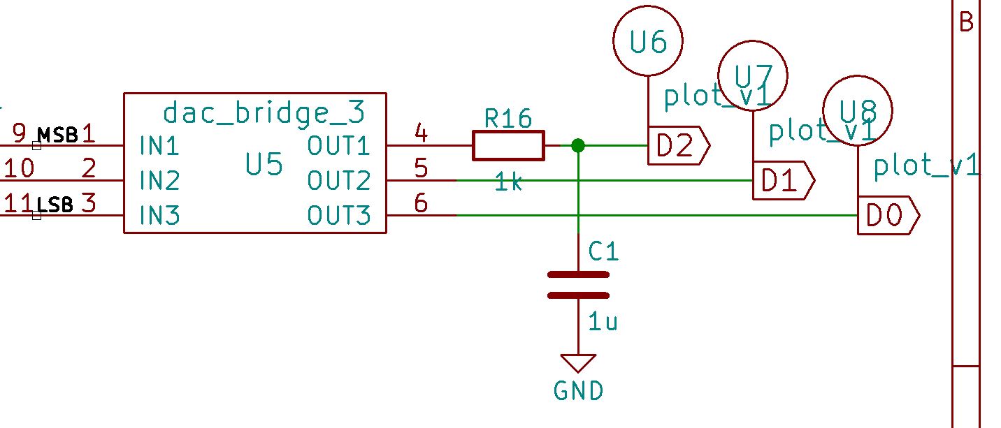
Below is the schematic plotted on Eeschemia
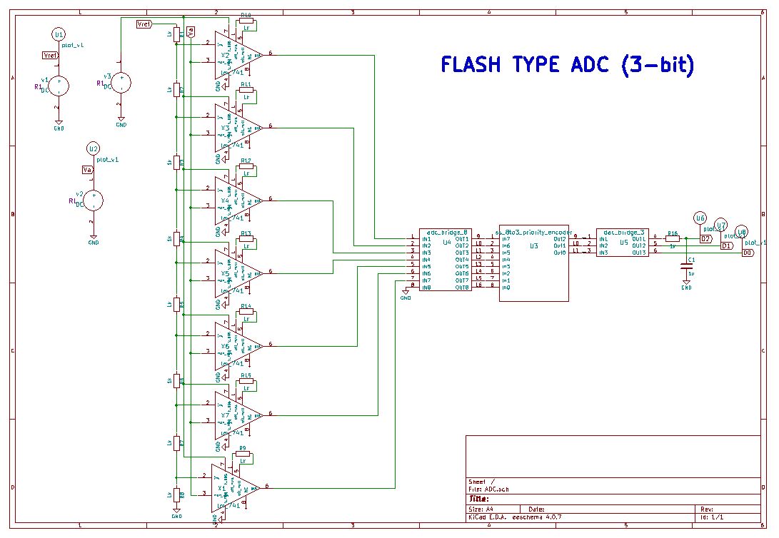
As we can see here, 7 instances of op-amp has been created, every op-amp's non-inverting input is connceted to input voltage so that if input voltage is greater than ladder resp. voltage, that op-amp will set to +VSat. Conversly, every op-amp's inverting input is connected to resp. ladder voltages so that if input voltage is less than ladder resp. voltage, that op-amp will set to -VSat.
At next stage, the ADC bridge will convert resp. analog voltages to digital form i.e. 0s & 1s. Further, the model of 8:3 encoder that has been created by NgVeri has instanced which will convert the outputs of resp. op-amp into binary form.
https://github.com/Sumanyu-Singh/Mixed-Signal-Design-of-3-bit-Flash-Type-ADC/tree/main/Netlists
For output testing I have taken Vref as 5v and Va as 5v. Also positive supply is 5v. So, voltages at inverting terminal of all the comparators are less than the inverting terminal voltage(i.e 5V) due to voltage divider circuit. So, output of all 7 comparators will be logic high (5v). Hence all the output digital bit will be high(logic-1 i.e 5).
Sumanyu Singh, Mtech (Microelectronics), Indian Institute of Information Technology, Allahabad, U.P, 211015
-
Kunal Ghosh (Co-Founder, VLSI System Design Pvt. Ltd.)
-
FOSSEE, IIT Bombay
-
Steve Hoover (Founder, Redwood EDA)
-
Sumanto Kar (eSim Team, FOSSEE, IIT Bombay)
[2] CMOS Analog Circuit Design Phillip E. Allen and Douglas R. Holberg.
[3] Verilog HDL: A Guide to Digital Design and Synthesis by Samir Palnitkar.