Programmable Systems-on-Chip (FPSoCs) are heterogeneous reconfigurable platforms consisting of hard processors and FPGA fabric. This repository contains experiments regarding the processor-FPGA transfer rates in Zynq-7000 devices. It serves as support to the paper "Performance Analysis of Processor-FPGA Communication in Low-Cost FPSoCs". Since data and figures were too many to fit in a single article all data is provided in this repository. The code used for the experiments is also provided.
Table of contents of this README file:
The repository is organized as follows:
- This README file contains explanation of the experiments. For each experiment a summary of the results and the more important plots are provided. The reader can also find a links to the code used for each experiment and a link to the full set of numeric results.
- code/: contains all programs used to do the experiments. A README file explaining the code and how to compile and run each program is provided inside their corresponding folders.
- fpga-hardware: Vivado hardware projects for the FPGA, used to perform the experiments.
- results/: contains all numeric results for the experiments.
- figures/: contains the figures used in the README files in this repository.
To make use of this repository download it as a zip or install git in your computer and download it using:
# navigate to the folder where you want to download the repository
git clone https://github.com/UviDTE-FPSoC/Zynq7000-time-measurements.gitA simplified block diagram of Zynq-7000 is depicted in the figure below. Zynq-7000 architecture consists of a Processing System (PS) and Programmable Logic (PL) in form of FPGA in a single chip, coupled by high throughput datapaths.
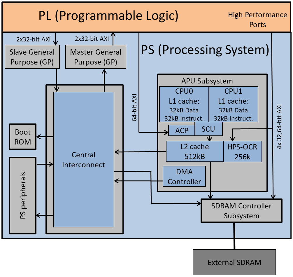
The Processing System (PS) features a application processor unit (APU), 64kB on-chip RAM (PS-OCR), booting ROM, SDRAM controller (SDRAMC), DMA controller (DMAC), and PS peripherals (such as Ethernet and USB controllers, UARTs, and timers). The APU includes two ARM Cortex-A9 32-bit processors, with 32kB L1 data cache and 32kB L1 instruction cache each and 512kB L2 shared instruction and data cache. A Snoop Control Unit (SCU) ensures coherency among L1 caches, L2 cache, and SDRAM contents.
Central Interconnect is a partially connected crossbar switch interconnecting all elements in the PS. All interconnection elements in PS are AXI4-compliant.
Interconnection resources between the HPS and the FPGA fabric can be divided in two groups:
- Those through which HPS accesses FPGA as master:
- 2 Master General Purpose (GP) bridges, buses whose data width is 32-bit (referred to as GP0 and GP1 in the reminder of the repository).
- Those through which FPGA accesses HPS as master:
- 2 Slave General Purpose (GP) bridges, bus enabling FPGA masters to access HPS peripherals, DMAC, and SDRAMC.
- ACP port. It permits masters in FPGA to access cache memory in a coherent way. ACP width is 64-bit.
- FPGA-to-SDRAM high performance ports configurable master ports, which access the external SDRAM memory in a non-coherent way directly through SDRAMC. Configurable width to 32- or 64-bit.
These experiments represent the core of PS-PL transfer rate measurements when using the HPS as master to move data. They provide a good overview of the device behaviour. Experiments are performed using Linaro Operating System and Baremetal. Baremetal measurements provide the fastest data rates that can be achieved in the device. These data can be compared with transfer speed achieved when using OS to observe OS effect on transfers. All design parameters that have been identified to influence transfer rate are considered, with the exception of processor workload, which is kept to a minimum. The reason for this is that it is not practically feasible to consider the many different combination of tasks that the processors may be executing in real applications. Taking into account just a subset of those would result in partial and likely misleading conclusions, difficult (if at all possible) to be extrapolated to specific applications. Therefore, the results of the experiments presented in next section represent the optimal performance under each tested scenario, which is reduced as processor workload increases.
To perform transfers to PL an On-Chip RAM (FPGA-OCR) was located in the FPGA simulating any possible peripheral to transfer data with. The FPGA-OCR is connected to one of the HPS-to-FPGA bridges (where HPS acts as master), in this case GP1. The board used was a Zedboard.
Transfer rates between HPS and FPGA when HPS is the master are measured for different combinations of values of the following parameters:
- OS or baremetal implementation:
- Application running in Linaro, an Ubuntu distribution.
- Baremetal application running in one of the ARM cores.
- Master starting AXI bus transfers:
- CPU: one of the ARM cores controls data transfer. The program code/Baremetal/PS-to-PL_CPU_GP1 is used for baremetal and code/Linaro_OS/PS-to-PL_CPU_GP1 for Linaro OS.
- DMAC: HPS DMA Controller (PL330) executes data transfer microcode in PS-OCR, freeing the processor from this task. The program code/Baremetal/PS-to-PL_PL330DMAC is used for baremetal and code/Linaro_OS/PS-to-PL_PL330DMAC for Linaro OS.
- Bridge. All bridges having HPS as master have been tested. In this case there is only one type: GP. GP1 has been used during the experiments.
- Cache enablement:
- Caches off. All memory accesses are to external SDRAM. Caches were not switched off for Linaro since it does not make much sense. Doing it in baremetal is enough to measure the effect of caches in the execution of transfer rate programs. To switch ON or OFF the caches set to 9 or 0 the macro CACHE_CONFIG in the configuration.h file of each program.
- Caches on. Accesses are to L1, L2, or external SDRAM, depending on where data are located and the port used.
- Coherency (only applies for DMAC): DMAC can access PS memories through ACP (coherent access) or directly access external SDRAM through the SDRAMC port from Central Interconnect (non-coherent access). In the baremetal tests coherency is automatically changed depending on cache enablement. When cache is OFF non-coherent access is applied (coherent access will be slower because the access would be Central Interconnect->L2->SDRAM) so it is better to directly do non coherent Central Interconnect->SDRAM). When cache is ON the access is non-coherent (through Central Interconnect->SDRAM port) or coherent (to cache).
- Preparation of DMA microcode program (only applies for DMAC). In most applications the size of the transfer and the address of the destiny and source buffers is known before the transfer takes place so the DMAC microcode programs can be prepared beforehand (during board start-up and initializations) and its preparation time can be saved when the program is actually running the application-ralated tasks. For both, baremetal and OS the transfer time is measured without DMAC microcode preparation time.
- Data size from 2B to 2MB, in 2x steps. This automatically done by the program that repeats the measurements for every data size.
- FPGA frequency from 50 to 250MHz, in 50MHz steps. For tests failing at 200MHz, the frequency was reduced in 20MHz steps until correct operation was achieved.
Tests are repeated 100 times (automatically done by the application) and mean value is given as result.
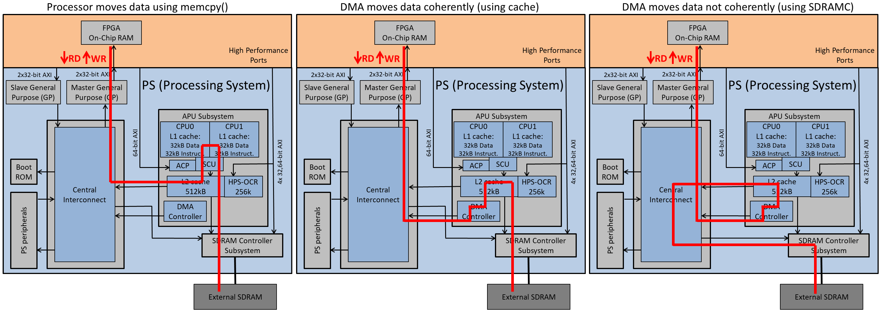
These are the data paths depending on AXI master (CPU or DMA) and coherency (using cache or directly accessing SDRAMC):
The full set of numeric values for the main experiments is in results/Zynq7000_HPS-FPGA.xlsx.
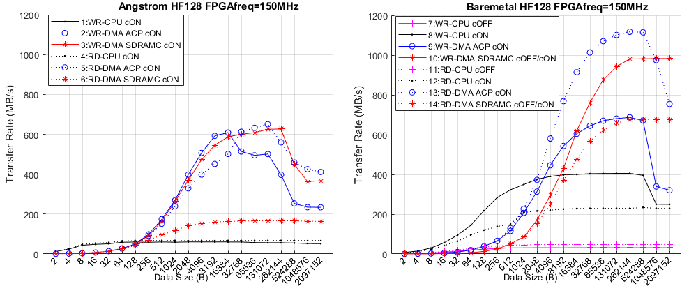
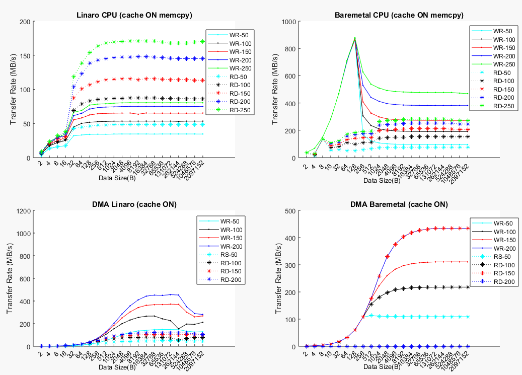
The best performance is achieved, as expected, when FPGA frequency is higher and the cache is enabled. In Zynq-7000 the maximum frequency all experiments correctly run is 200MHz. In Cyclone V SoC this frequency is 150MHz. One reason for this is that the OCR used in the FPGA is bigger in Cyclone V SoC. To be able to more easily compare the two devices the main results for Xilinx are presented for 150MHz too, knowing that faster data rates are available in Zynq7000_HPS-FPGA.xlsx file. The following figure shows the data rates at 150MHz in Zynq-7000 depending on data size, master starting the transfers (CPU or DMA) and data direction (WR or RD). Measurements with CPU as master in this figure are carried out with the memcpy() method. Measurements with the forloop() method are always slower and are not plotted. This graph is equivalent to the the main figure for for Cyclone V SoC.
Transfer rate (in MB/s) of experiments through GP1 bridge with FPGA frequency 150MHz
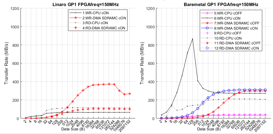
The shape of most of the plots for Zynq-7000 is the same as the plots for Cyclone V SoC. At the beginning the transfer rate grows fast as the initialization time becomes smaller with respect to the transfer time. When this effect becomes negligible plots become flat. The experiments involving cache suffer a reduction above 32kB (size of cache L1) and 512kB (size of cache L2) due to cache overflow.
When analizing the Zynq-7000 and Cyclone V SoC figures it can be noticed that there are some differences in the transfer rates of these devices. When using OS Cyclone V SoC results faster than Xilinx when using DMA (33% in WR and 27% in RD) but slower when using CPU (5.5% in WR and 56% in RD). In Baremetal plots a similar situation happens. Cyclone V SoC is faster when using the DMAC through SDRAMC (38% in WR and 65% in RD) but slower when moving data using the CPU (18% in WR and 2.5% in RD). Therefore it can be stated that in general terms both platforms are similar, being Zynq-7000 faster in HPS-to-FPGA transfers when CPU is used and Cyclone V SoC when DMAC is used.
The effect that the FPGA frequency has in the HPS-to-FPGA transfer rate are plotted in the following figure:
The reduction provoked by the frequency is summarized in the following Table. It shows the transfer rate reduction (%) in GP bridge when lowering the FPGA operating frequency from 150MHz in Zynq-7000.
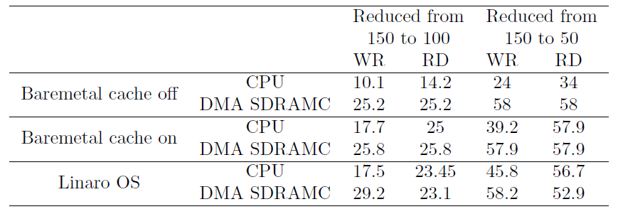
The behaviour is very similar to that of the Cyclone V SoC, shown in table. The FPGA frequency has more effect on Zynq-7000, especially in methods using the CPU and the RD direction.
The selection of the best AXI master (CPU or DMAC) for an specific application depends on the implementation (OS or baremetal) and the data size. The following Table summarizes the fastest AXI master for each implementation and data size, extracted analyzing Figure in General Analysis of the Results.
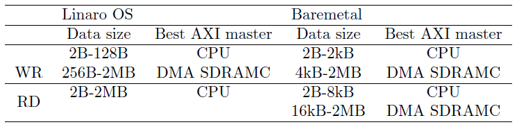
When using OS in WR the processor is the fastest for small data sizes and the DMAC for bigger ones. This is the same behaviour observed in Cyclone V SoC. However in RD the CPU is always faster than the DMAC. The reason is the double copy (from FPGA to intermediate buffer in the driver to the application space) needed when using OS. In Cyclone V SoC the bigger HPS-to-FPGA bridge available compensates this drawback and makes the DMAC clearly faster. In baremetal the same behaviour observed for Cyclone V SoC is observed. CPU is faster for small data sizes and DMAC for bigger ones.