This article describes the major changes that have been made in GPGPU-Sim version 4.x. If you are not familiar already with GPGPU-Sim, please see the original GPGPU-Sim ISPASS paper, GPGPU-Sim 3.x tutorial, videos and GPGPU-Sim 3.x manual.
If you use GPGPU-Sim 4.x in your research, please cite:
Mahmoud Khairy, Zhensheng Shen, Tor M. Aamodt, Timothy G. Rogers,
Accel-Sim: An Extensible Simulation Framework for Validated GPU Modeling,
in 2020 ACM/IEEE 47th Annual International Symposium on Computer Architecture (ISCA)
In the new version of GPGPU-Sim 4.x, we make extensive modifications to GPGPU-Sim 3.x’s performance model in order to accurately model contemporary and future GPU generations. We designed the new model to be highly flexible and not tuned to a specific architecture.
We made major changes at both the Streaming Multiprocessor (SM) core, caches and memory subsystem modeling.
- SM Core Model:
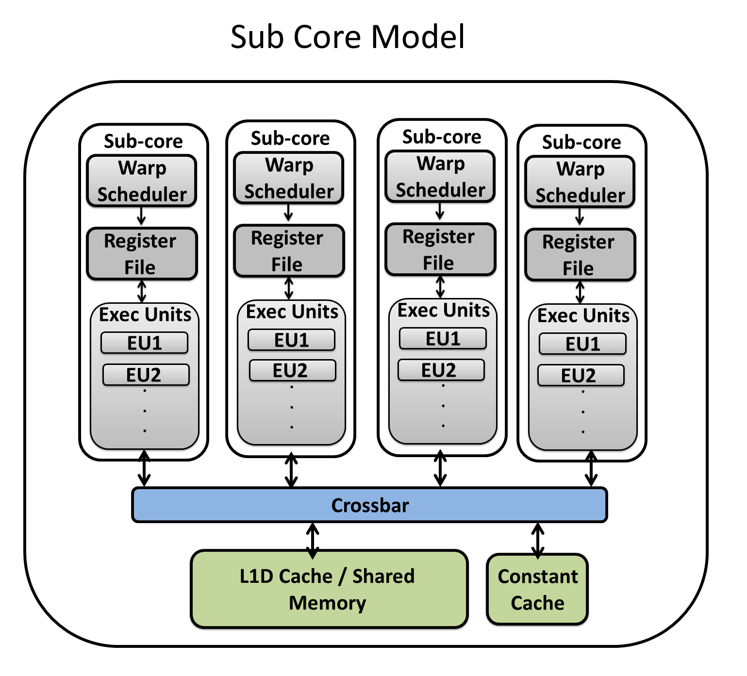
In the new core model, we increased the flexibility to model contemporary and future GPU generations. For example, we are able to model the kepler’s shared core model where warp schedulers are sharing the execution units and register file. Also, the new core model is flexible enough to build the Volta subcore model, where warp schedulers are isolated each scheduler has its own register file and exeuction units and only share the L1 cache and shared memory, as shown in the Volta whitepaper.
To enable sub_core model, you need to set sub_core model in the config file:
# Volta has sub core model, in which each scheduler has its own register file and EUs
# i.e. schedulers are isolated
-gpgpu_sub_core_model 1
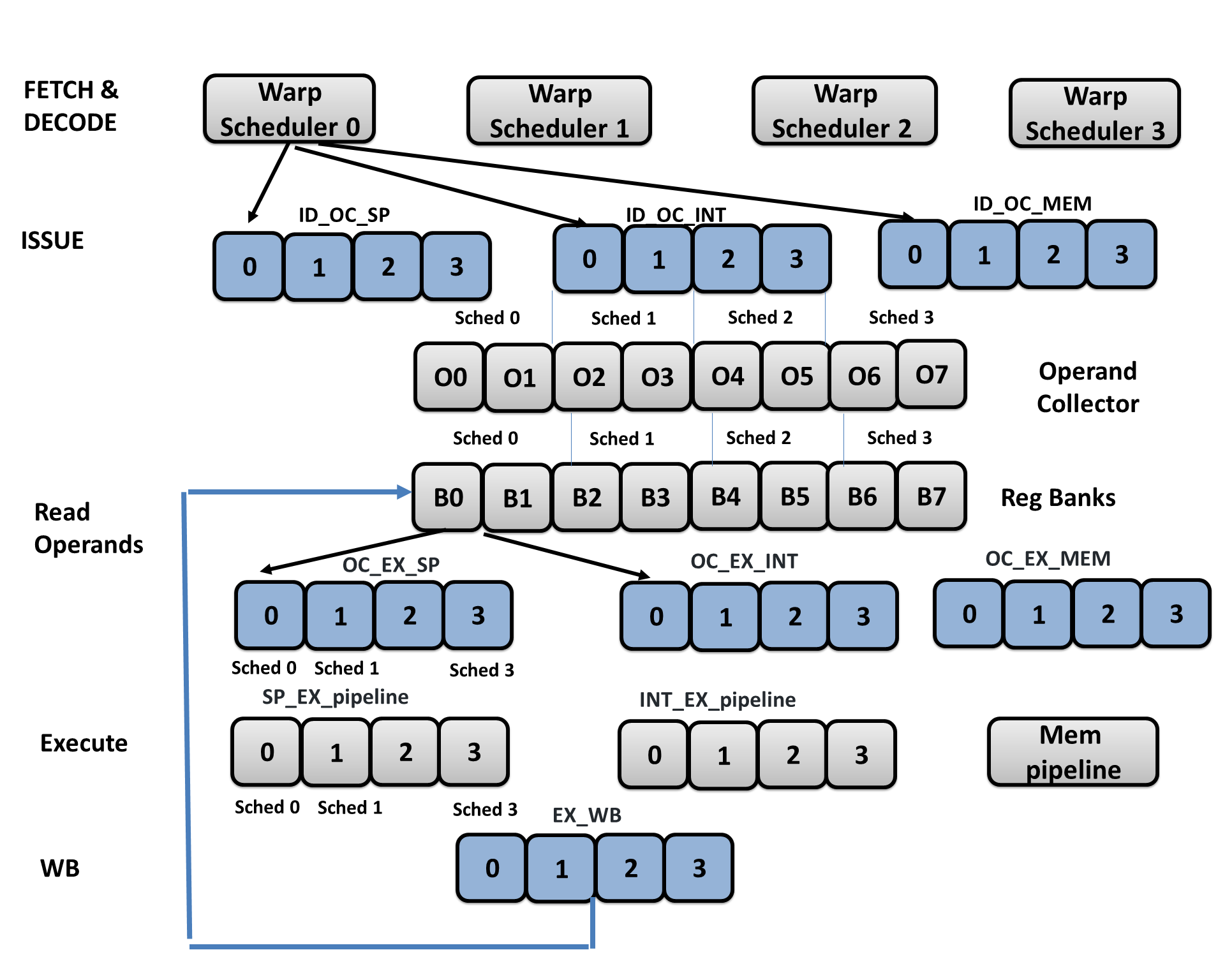
In sub_core model, warp schedulers are restrictively partitioned the pipeline, and each has its own register file, operand collectors, execution unit, and pipeline registers as shown in the below image:
Also, in trace-driven mode, we provide the flexibility and ability to add new execution units without the need to update the codebase. This ensures that when GPU vendor adds new domain-specific execution unit, such as tensor cores as in Volta or unified data path (UDP) as in Turing, we can adapt our model to this and add the new execution unit very quickly. To add a new specialized unit, the user declares the new unit in the configuration file as shown below and maps the machine ISA op codes that use this unit in the ISA def file. See an example of ISA Def file here.
# We support up to 8 specialized units defined in GPGPU-Sim
# to add a new unit, for example, tensor cores
# configuration string: <enabled>,<num_units>,<max_latency>,<ID_OC_SPEC>,<OC_EX_SPEC>,<NAME>
-specialized_unit_3 1,4,8,4,4,TENSOR
-trace_opcode_latency_initiation_spec_op_3 8,4
- Caches:
Our GPU cache model supports sectored, banked L1 cache design. Our sector size is constant=32B, so for 128B cache line configuration, each cache line has 4 sectors. Example to define L1 sector cache with four banks:
# Add the 'S' character at the header as shown below; for non-sector cache design use 'N'
# cache configuration string: <sector?>:<nsets>:<bsize>:<assoc>,<rep>:<wr>:<alloc>:<wr_alloc>:<set_index_fn>,<mshr>:<N>:<merge>,<mq>:**<fifo_entry>
-gpgpu_cache:dl1  S:4:128:64,L:L:m:N:L,A:512:8,16:0,32

# 4 cache banks, we interleave 32B sector on each bank
-gpgpu_l1_banks 4
-gpgpu_l1_banks_byte_interleaving 32
Note well: When using sector cache ('S'), the sector size is hard-coded to 32 and the sector number is hard-coded to 4. Any value other than 128 passed to
bsizewill result in assertion error at run time!
In GPGPU-sim 3.x, L1 and shared latency was 1 cycle constant. To set different latencies:
-gpgpu_l1_latency 20
-gpgpu_smem_latency 20
L1 cache design can also be configured to be streaming. In the streaming cache, it allows many caches misses to be in flight (depending on MSHR throughput), regardless of how many cache lines are available in the cache set. This is very beneficial for streaming workloads, like memcpy, to not to be limited by cache size.
# Add the 's' character at the middle of cache configuration for streaming configuration, 'm' for ON_MISS and 'f' got ON_FILL
# cache configuration string: <sector?>:<nsets>:<bsize>:<assoc>,<rep>:<wr>:<alloc>:<wr_alloc>:<set_index_fn>,<mshr>:<N>:<merge>,<mq>:**<fifo_entry>
-gpgpu_cache:dl1  S:4:128:64,L:L:s:N:L,A:512:8,16:0,32
Contemporary GPU architectures make use of an adaptive cache mechanism, in which the device driver transparently configures the shared memory capacity and L1D capacity on a per-kernel basis. Using the adaptive cache, if a kernel does not utilize shared memory, all the onchip storage will be assigned to the L1D cache
# Assume defualt config is 32KB DL1 and 96KB shared memory
# In adaptive cache, we assign the remaining shared memory to L1 cache
# If the assigned shd mem = 0, then L1 cache = 128KB

# Volta adpative cache configuration example:
# Enable adaptive cache
-gpgpu_adaptive_cache_config 1
# Define shmem size options
# For more info, see https://docs.nvidia.com/cuda/cuda-c-programming-guide/index.html#shared-memory-7-x
-gpgpu_shmem_option 0,8,16,32,64,96
# Max L1+shd mem = 128KB
-gpgpu_unified_l1d_size 128
We support sub-sector fetch-on-read write design with true write-allocate modeling for both L1&L2 caches. The new policy conserves memory bandwidth when running a write-intensive GPU workload. When a write to a single byte is received, it writes the byte to the sector, sets a corresponding write bit in a byte-level write mask, and sets the sector as valid and modified. When a sector read request is received to a modified sector, it first checks if the sector write-mask is complete, otherwise, it generates a read request for this sector. In Volta cards and above, L1 cache is write_allocate write_through, and L2 cache is write_allocate write_back. For the L1 cache, we specify the percentage of L1 size dedicated for write to mitigate read-write interference.
# To use sub-sector lazy_read design, use character 'L', 'N' for no write allocate, 'W' for naive write design found in GPGPU-sim 3.x and 'F' for fetch-on-write
# cache configuration string: <sector?>:<nsets>:<bsize>:<assoc>,<rep>:<wr>:<alloc>:<wr_alloc>:<set_index_fn>,<mshr>:<N>:<merge>,<mq>:**<fifo_entry>

# configure L1 write_allocate lazy_fetch 'L' with write_through 'T' policy as in Volta
-gpgpu_cache:dl1  S:4:128:64,L:T:m:L:L,A:512:8,16:0,32
# Set 25% of L1 size for write
-gpgpu_l1_cache_write_ratio 25

# configure L2 write_allocate lazy_fetch 'L' with write_back 'B' policiy as in Volta
-gpgpu_cache:dl2 S:32:128:24,L:B:m:L:P,A:192:4,32:0,32
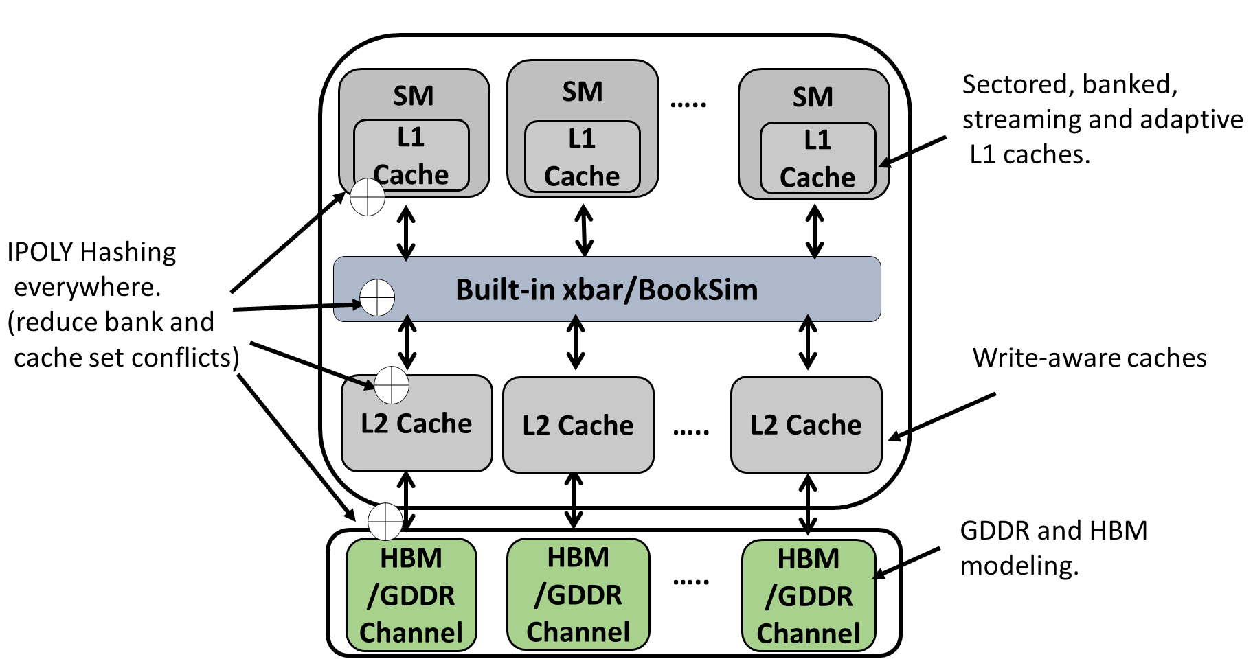
We added bitwise XORing and advanced polynomial hashing everywhere in the cache/memory system to reduce bank and cache set conflicts and thus alleviate contention. You can set different hashing functions at different levels of the memory hierarchy: L1 cache set hashing, L1 bank hashing, L2 cache bank hashing, L2 cache set indexing, and memory banks indexing.
# to select polynomial hashing function, use the character 'P', 'L' for linear indexing and 'X' for bitwise XORing
# cache configuration string: <sector?>:<nsets>:<bsize>:<assoc>,<rep>:<wr>:<alloc>:<wr_alloc>:<set_index_fn>,<mshr>:<N>:<merge>,<mq>:**<fifo_entry>

# set L1 cache set index to linear
-gpgpu_cache:dl1  S:4:128:64,L:L:s:N:L,A:512:8,16:0,32

# set L1 bank index to linear
# 0:linear, 1:xoring, 2:polynomiay
-gpgpu_l1_banks_hashing_function 0

# set L2 cache set index to polynomial
-gpgpu_cache:dl2 S:32:128:24,L:B:m:L:P,A:192:4,32:0,32

# set L2 cache bank index to polynomial
# 0:linear, 1:xoring, 2:polynomial, 3:PAE, 4:RANDOM
-gpgpu_memory_partition_indexing 2

# set dram bank index to linear
-dram_bnk_indexing_policy 0
# select lower bits for bnkgrp to increase bnkgrp parallelism
-dram_bnkgrp_indexing_policy 1
See hashing.cc for further details about hashing function implementation.
- Interconnect:
We developed a fast built-in xbar interconnect instead of the complex Booksim-based xbar so the user can have more control and understanding of the interconnect. The user can switch between the built-in xbar and Booksim interconnect. The built-in xbar is a standard crossbar with iSLIP arbitration. For more details, see local_interconnect.cc.
# interconnection
#-network_mode 1
#-inter_config_file config_volta_islip.icnt
# to use built-in local xbar
-network_mode 2
-icnt_in_buffer_limit 512
-icnt_out_buffer_limit 512
-icnt_subnets 2
-icnt_flit_size 40
-icnt_arbiter_algo 1
- Memory Model:
In the memory system, we model new advances in HBM and GDDR6. This includes the dual-bus interface to launch row and column commands simultaneously, increasing bank parallelism, and detailed HBM timing. Further, we implement well-known memory optimization techniques such as advanced xor-based bank indexing and separate read/write buffers, to reduce memory bank conflicts and read-write interference.
# HBM configuration example:
-gpgpu_n_mem_per_ctrlr 1
-gpgpu_dram_buswidth 16
-gpgpu_dram_burst_length 2
-dram_data_command_freq_ratio 2  # HBM is DDR

# Timing for 850 MHZ
-gpgpu_dram_timing_opt "nbk=16:CCD=1:RRD=3:RCD=12:RAS=28:RP=12:RC=40:
                        CL=12:WL=2:CDLR=3:WR=10:nbkgrp=4:CCDL=2:RTPL=3"

# HBM has dual bus interface, in which it can issue two col and row commands at a time
-dram_dual_bus_interface 1

# to enable write queue
-dram_seperate_write_queue_enable 1
# write_queue_size:write_high_watermark:write_low_watermark
-dram_write_queue_size 64:56:32