Welcome to the PCI2Nano Reference Platform repo. In this repo you'll find an inexpensive suggested Reference Platform for designing and testing PCI functions on a DE0-Nano FPGA to an x86 host. I have personally built/connected/tested every single one of these components and can confirm they work for fast iterative PCI development.
The design collateral that is included with this repo are the kicad design files for the PCI2Nano breakout board and a Quartus project that contains all the correct PCI pinout constraints for the PCI2Nano breakout board. This repo does not contain an actual PCI core written in verilog. For an example PCI core implementation with a UART check out the PCI2Nano-RTL repo here: https://github.com/defparam/PCI2Nano-RTL/
This work is licensed under a Creative Commons Attribution-ShareAlike 4.0 International License.

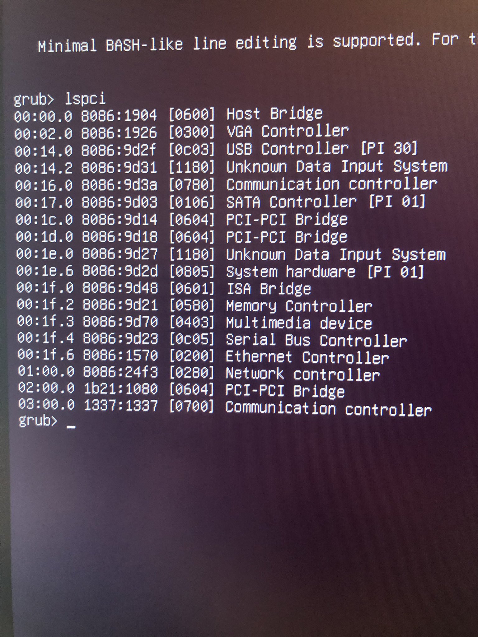
My l337-Communication Controller
| Part | Description | Price |
|---|---|---|
| DE0-Nano | FPGA Board | ~$100.00 |
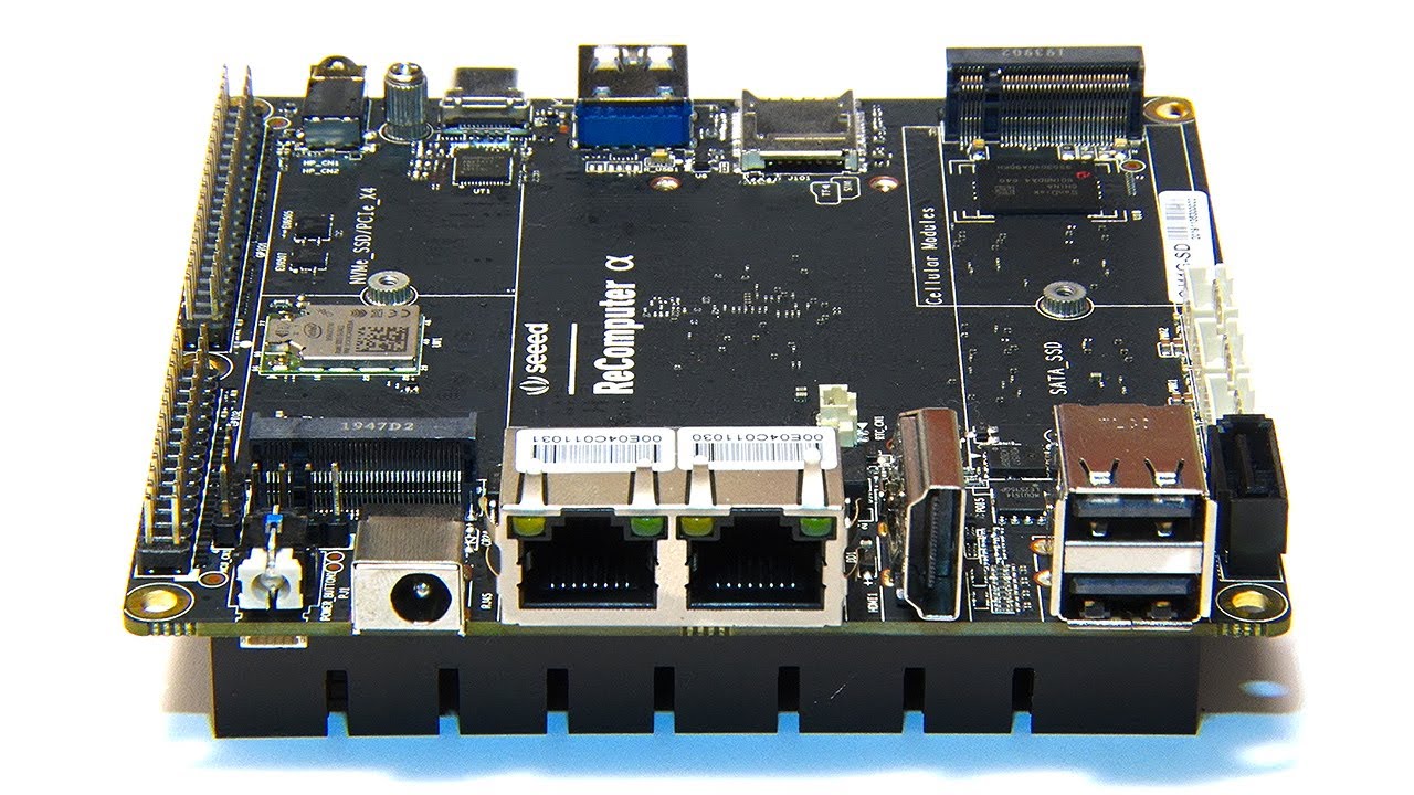
| Seeed Odyssey X86J4105 SBC | SIngle Board Computer | ~$185.00 |
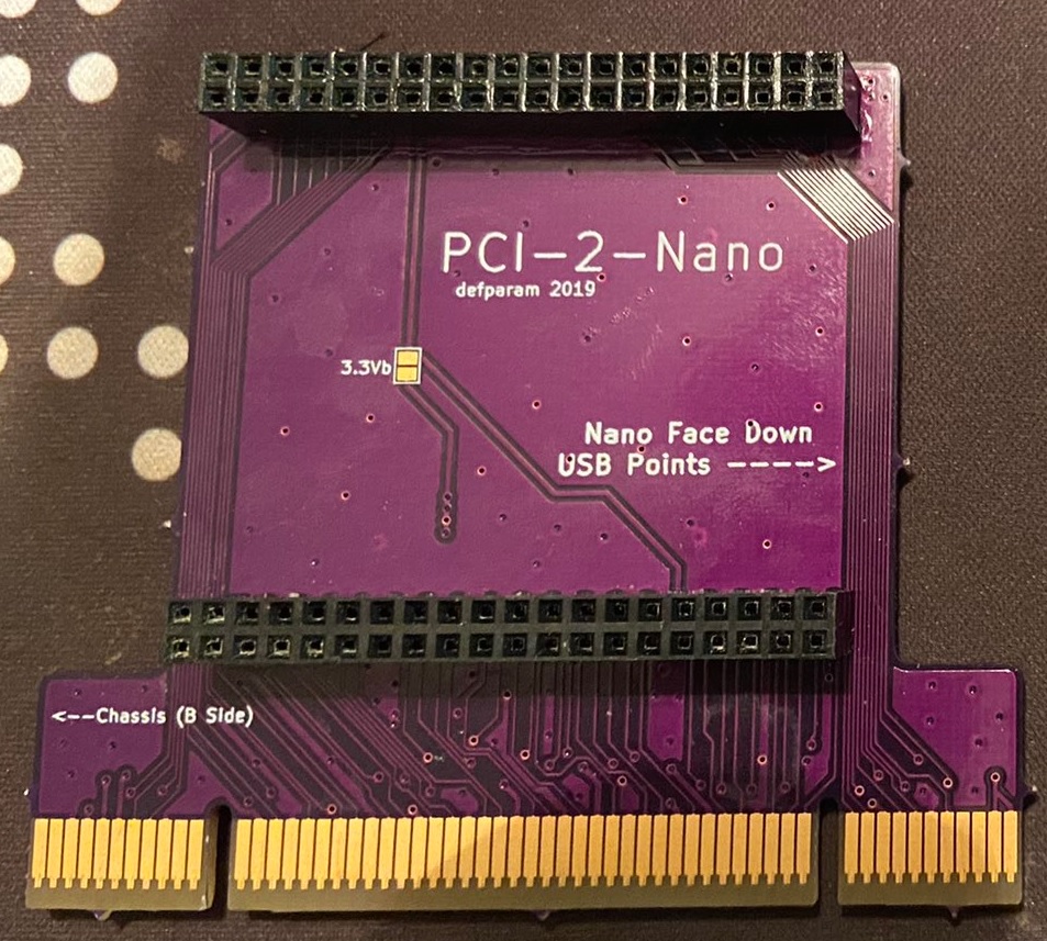
| PCI2Nano Breakout PCB | Coverts PCI to DE0-Nano GPIO | ~$45 (OSHPark for 3) |
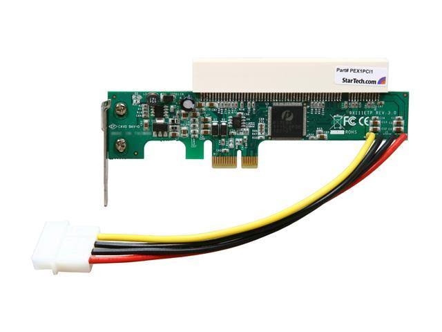
| Startech PEX1PCI1 | Converts PCIe to PCI | ~$40 |
| M.2 Key M Extender PCIE x16 | Break out M.2 to PCIe x16 | ~$32 |
| 2x 100mil 40-pin IDC sockets | Soldered to the PCB | ~$1-$2 |
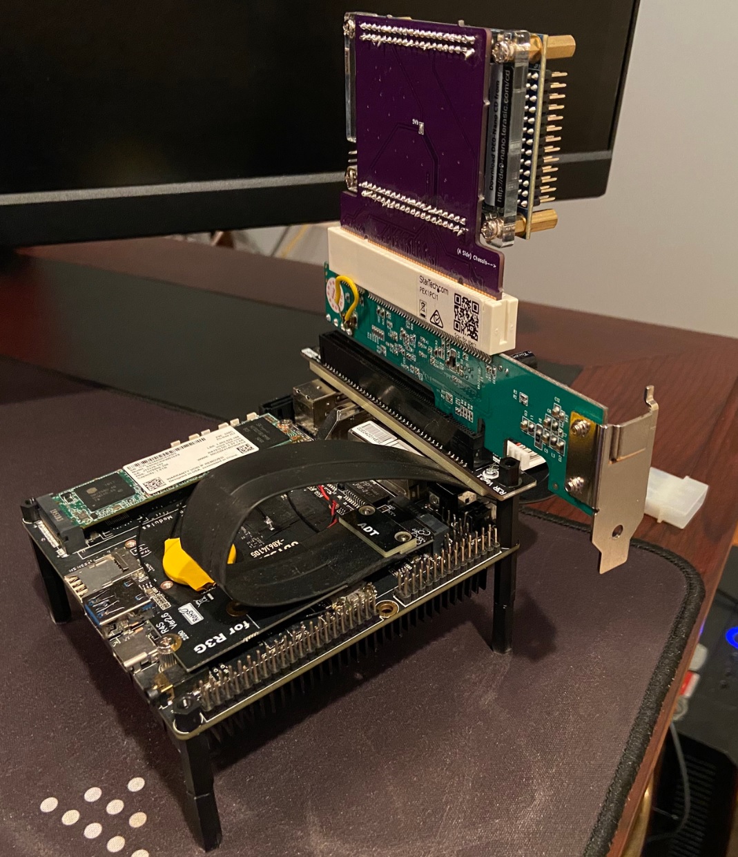
- Mount the Extender cable into the Odyssey M.2 M Key slot. If you have standoffs you can affix the x16 connector of the extender to the SBC as shown in the picture above.
- Mount the PEX1PCI1 onto the x16 connector. Supplying the molex power I believe is not required since it is used to power the 5V rails of a mounted PCI device, the PCI2Nano doesn't use this 5V rail (unless you bridge it to the Nano's 5V GPIO power pin via the board shunt). However it is best to power the nano through its USB cable
- Connect the PCI2Nano breakout board to the DE0-Nano, make sure that the USB of the nano points in the correct direction as specified by the silkscreen
- Connect the PCI side of the PCI2Nano onto the PEX1PCI1, make sure it is connected in the orientation as indicated by the silk screen. The arrow indicating the chassis side should be pointed to the externel side of the PEX1PCI1
There is a small amount of soldering involved with the PCB board to connect the 100mil IDC socket to the PCB board.
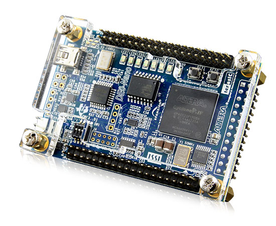
The DE0-Nano:
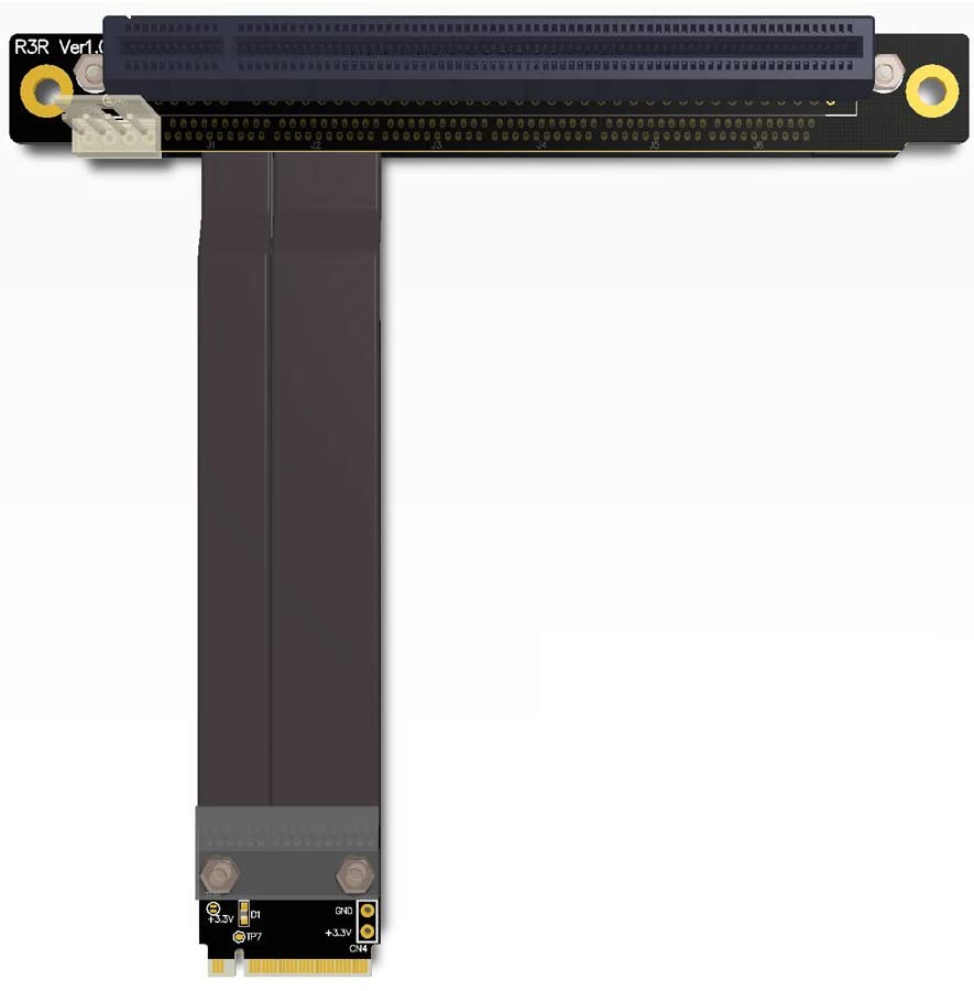
The PCI2Nano PCB:
The PEX1PCI1 PCIe-2-PCI Bridge:
The Seeed Odyssey X86J4105 SBC:
The M.2 Key M Extender PCIE x16: