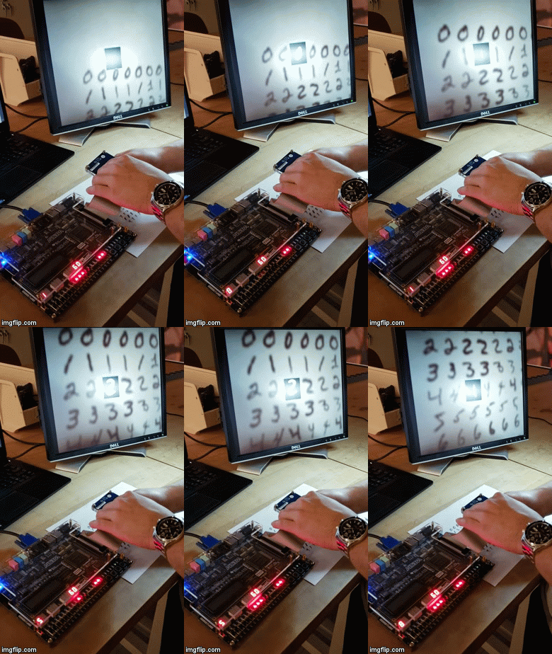
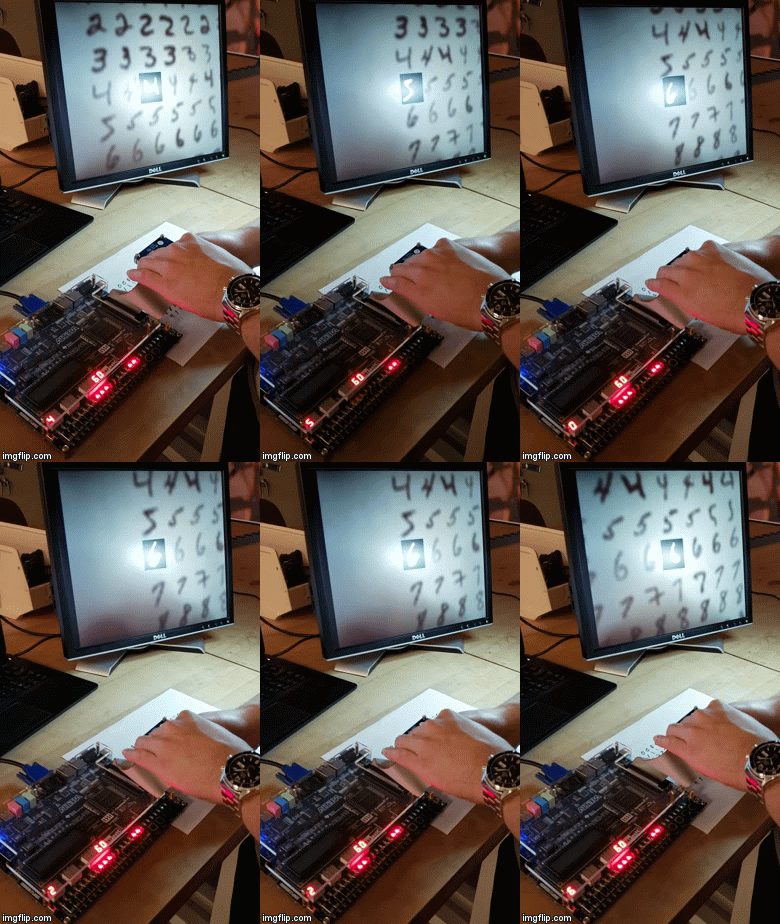
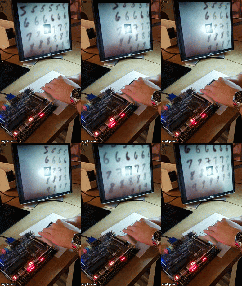
| Demo Pt. 1 | Demo Pt. 2 | Demo Pt. 3 |
|---|---|---|
 |
 |
 |
Thank you for viewing my project. My write-up about the project is divded into four parts: A high-level introduction, hardware description, descriptions of each file, and build instructions. Please email me with any questions/comments at grantyu2020@u.northwestern.edu.
Section I. High-Level Introduction
Over the past decade, we have witnessed a major boom in the deep learning space, as an increasingly large number of applications are adopting inference-based solutions. A major subcategory of problems within the deep learning space is image classification, which is widely used in real-time embedded applications. Such systems require high performance and low power consumption, targets which can be achieved by using specialized computing platforms, such as field-programmable gate arrays (FPGAs). This paper discusses a low-power implementation of a convolutional neural network (CNN) on the Intel Cyclone IV FPGA to perform the task of handwritten digit classification. A sliding window buffer is implemented using the FPGA fabric and on-chip memory to minimize energy-expensive off-chip memory accesses, and a small, optimized GPU-like multiplier-accumulator (MAC) core computes all of the activation layers. This implementation uses less than 50% of the Cyclone IV FPGA’s total area and costs $488.
Section II. Hardware Description
The hardware used in this project include the Terasic DE2-115 Development Board, the Terasic D8M-GPIO Camera Module, and a generic VGA monitor. The heart of the hardware system, the DE2-115, is a general purpose FPGA breakout board designed for university programs. The on-board FPGA is the Intel Cyclone IV EP4CE115. The logic fabric inside of the Cyclone IV would be reconfigured to meet the target I/O requirements of the design; it should take in an input image stream of handwritten digits and compute the most accurate classification of the captured digit. The image stream as seen by the D8M-GPIO image sensor would be shown on a VGA monitor with a green-box-delineated region for the valid portion of the frame. In order to configure the FPGA to address the classification challenge, we use a hardware descriptive language (HDL). For this project, we choose SystemVerilog HDL to synthesize all of the necessary hardware blocks.
At the heart of the design is the MAC_ARRAY, a parallel array of pipelined multipliers and adders. The MAC_ARRAY is central to the two-dimensional convolutions that are needed for CNN inferences. Inferencing is composed of a number of linear operations combined with nonlinear activation functions between each layer, and all of these operations are fundamentally necessary in creating distinctions between training features. To calculate the convolutional and pooling feature maps, our hardware needs to be able to perform fast linear operations. Many FPGAs provides optimized hardware primitives such as DSP tiles, which are dedicated logic blocks that are already fabricated within the chip. The Intel Cyclone IV FPGA used in this project contains 266 embedded 18x18 multipliers, which would work perfectly for deep learning inferencing. Therefore, we see that another advantage of using FPGAs is that these fast, optimized DSP blocks are ready to use out-of-the-box, saving the designer ample time. The interface between the designer and these DSP tiles would simply be the designated multiplication operator in the HDL or high-level synthesis tool.
Because the goal is to minimize power and area costs, we choose to use a relatively tiny MAC array that consists of 144 multipliers and 128 adders. These multipliers and adders are organized into distinct pipeline stages, with the input weights and activation data streaming into the multiplier stage first, and then into a number of stages for the adder tree. Popular choices of resolution for neural network accelerators are 8 bits and 16 bits (and it is worth mentioning that as of recent, binary neural networks (BNNs) have shown good promise). Using a 16 bit resolution would result in greater area usage than 8 bits. More RAM would be needed, as well as larger multipliers and adders. Despite these drawbacks, we choose to use a 16 bit resolution in this project for a better quality of performance. These 16-bit computations are implemented in fixed-point.
The CNN architecture used is a 7-layer network, as shown below. Our input MNIST image is 30x30. The original dimensions of MNIST sample images are 28x28, but we used 30x30 so that every convolutional kernel in the network can be restricted to a 3x3 size. All original MNIST images have been padded on the edges with the color black (pixel value of 0x00). A 3x3 convolutional kernel transforms the input layer of 30x30 pixels into 16 feature maps of 28x28 pixels. Then, the rectified linear unit (ReLu) activation function is applied (nonlinear transformation). The next 3 layers follow a similar pattern. The last two fully connected layers generate a 64x1 vector in the penultimate layer and the final 10x1 vector in the final layer. The max() function is then applied to the 10x1 vector to get the classification.
Classification simulation results are shown below.
We have seen how the activation layer computations are implemented in hardware; now, we look into how we schedule, send, and receive pixel and feature map data between the image sensor, the block memory, and the MAC array. The D8M-GPIO captures raw CMOS CCD data and processes it using Terasic’s provided hardware drivers, including a MIPI interface module, auto-focus module, and RGB conversion module. Terasic’s hardware drivers and other starter code can be found within a demo folder on their website [8]. The demo code also uses a VGA driver to interface with the DE2-115’s outbound VGA port, which would be connected to the VGA monitor. Therefore, the hardware for this project needs to intercept the outgoing 24-bit RGB data (to VGA output), process the data, and send out new electrical signals to the VGA output as well as the 7 segment display.
After the incoming image stream is intercepted, processing occurs in the following order: convert the incoming image into a contour map (for easier MNIST classification), and check if the pixel falls within the valid subwindow for classification. If that is true, we set a strobe signal high to indicate that the pixel is valid. Valid pixels are counted as valid input layer data to the sender’s state machine.
A novel technique introduced in this project is the sliding window line buffer in the CNN_SENDER module. The CNN_SENDER module contains a finite state machine controller for memory reading and data transfer to the MAC array. Reads targeted towards the main memory bank tend to be expensive and costly, especially for the fully connected layers of CNNs and architectures like the multilayer perceptron (MLP). A line buffer in the form of a 3x3 register array window and 2 block RAMs for row storage is used to read in the image pixel-by-pixel. Due to the spatial locality of data processing for CNN feature maps, our 3x3 register array acts as a cache to remember the data that we need for the first layer convolution. Therefore, for each convolutional kernel for a 3x3-sized window, we only need one memory read, instead of nine.
In general, the hardware system outlined above shows potential usage for:
● Researchers who would like to accelerate machine learning algorithms for image classification
● Hardware designers who need a reference to a working system involving machine learning
● Students in machine learning or FPGA design seeking to learn HDL techniques for machine learning
Section III. Design File Descriptions
(All design files are licensed under the GNU General Public License v3.0)
DE2_115_D8M_RTL.sv: This is the top-level module and name of the Quartus Prime file used to synthesize the design. It contains all of the basic hardware drivers for the D8M-GPIO, VGA monitor, 7 segment display, and the main design itself.
mnist_classifer_top.sv: This is the preprocessing module that receives raw RGB pixels and VGA frame control signals. This preprocessing module organizes and instantiates several other components that control the VGA output stream, the 7 segment display decoder, and gets the contour of the image.
contour_draw.sv: This module facilitates the control signals, like X_VALID and Y_VALID, that draw a small contoured window on the output VGA monitor.
contour.sv: This module instantiates multiplexers and comparators to get the grayscale contour of the original RGB image.
cam2cnn.sv: This module is essentially a finite state machine controller that checks if pixels coming from the camera to the CNN are valid, and it does so by checking the strobe (valid) signal that is synchronized with the pixel signals.
segment7.sv: This module decodes a binary coded digit (BCD) into the correct visual display on the on-board 7 segment display.
RGB2GRAY.sv: This module converts RGB signals to a grayscale value (that is biased towards higher luminosity, for greater black-and-white contrast). The grayscale value is then used for contouring calculations.
mod_N_counter.sv: This module is a general counter IP.
top.sv: This is the top-level module for the CNN system itself, which contains the sender, receiver, state machine controllers, MAC array, line buffers, and weight/bias memories.
sram.sv: This is the basic unit of on-chip block RAM.
wt_fc_mem[0-7].sv: These 8 BRAM blocks all contain the weights needed for the first fully connected layer of the network.
wt_mem[0-7].sv: These are the 8 BRAM blocks that contain the weights for all other layers (separated out for optimal BRAM size allocation).
bi_mem0.sv: This single BRAM contains the biases for all of the layers.
controller.sv: This module is a subset of top.sv that separates out the sender, MAC array, and receiver away from the memory blocks themselves (for the purpose of easier testing).
line_buffer_group.sv: This module is a single BRAM block for two potential rows of an image frame (two rows make up a group).
ff_line_buffer_groups.sv: This module instantiates 16 groups of these line_buffer_groups for the 16 different feature map outputs of layer 1.
fmap_[I-III].sv: These memory blocks each store feature maps from different layers of the network.
cnn_sender.sv: This module contains an intensive finite state machine that performs all weight/bias memory reading operations, line buffering operations, and pipelining operations that feed pertinent data to the MAC array.
cnn_receiver.sv: This module contains an intensive finite state machine that facilitates the retrieval and memory storage demultiplexing for feature map outputs from the MAC array.
mac_array.sv: This module is the fabric of DSP tiles that perform all linear activation operations.
mac.sv: This module is the basic building block of the mac_array and is a primitive containing 9 embedded multipliers and 8 embedded adders (tuned to a 16-bit resolution).
IV. Build Instruction
-
The first step is to synthesize the hardware that will be configured onto the FPGA’s logic fabric. In order to do that, we will need the Quartus Prime software (the version used in this project is 18.1, and the Quartus Prime version is Lite). In the repository, there is a file called “DE2_115_D8M_RTL.qpf.” Open this file on Quartus Prime.
-
The entire project, with all of the SystemVerilog design files bundled up, should be contained under the “Files” section. Press the blue play button, “Run Compilation,” to synthesize, place and route, and assemble the hardware architecture. Once done, you should see the green checkmark.
Quartus Compilation Screenshot:
-
Open the “output_files” directory in the repository. Copy the file “DE2_115_D8M_RTL.sof” into the “demo_batch” directory.
-
The next step is to connect the D8M-GPIO to the DE2-115’s GPIO pins, VGA monitor to the DE2-115 via VGA cable, and connect the USB programming cable from your machine to the DE2-115. Power on the DE2-115 by connecting the power adapter to a wall socket.
-
On Window, run “test.bat” in the demo_batch directory. On Linux, modify the “test.sh” shell script so that your Quartus directories are in the right place. Then, run “test.sh.” The design should be transferred to the system now.


