This tool helps you to make pads for mutual capacitance method on Pcbnew application. If you use bitmap to component converter to make pads, you can not use DRC well. But this macro draws pads as zone, so you can use DRC to check design rules on your PCB.
This is just a tool to provide the easy way to make pad on PCB. No case, no additional hardware and no firmware are provided.
Decide parameters for pads yourself. Default parameters might be useless.
There are some restrictions:
- Only a type pad can be used on a single PCB design.
- Remove all elements before you change pad type.
- There are some test KiCAD project in this repository but do not try to reuse their design. They have never tested.
- Copy ESC_Pads.lib on your workspace and specify it to be used by the Eeschema.
- Copy ESC_Pads.pretty directory with its contents and specify they can be found by the Pcbnew.
- Draw circuit on Eeschema using symbols from ESC_Pads.lib.
- Bind between symbols and modules.
- Load nets into the Pcbnew.
- Layout modules on your own.
- Execute macro contained in the ESCP_Tool.py file.
- Add zone GND on your PCB.
- Execute DRC to make your PCB clean.
- Route between pads and between pads and components.
- Fill copper again or execute DRC if you required.
- Remove all elements add again if you move or rotate pad module.
See the following sections for more detail.
You can execute the macro through Pcbnew - Tools - Scripting Console. Execute clipboard content through context menu on the console if you use KiCAD 4.0.
If you use development version of KiCAD, helper tool: https://gist.github.com/hanya/08591a20a6c76bf9215f8175bd46681b
- Settings: you can load and store your parameter settings.
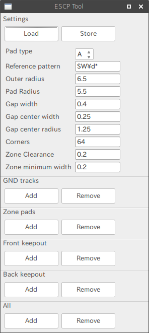
- Pad type: type of pad, choose this type to match with modules you have choosen.
- Reference pattern: regular expression pattern to be matched with your modules.
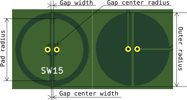
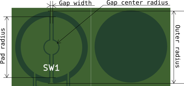
- Outer radius: radius of your pad.
- Pad radius: radius of inner pads.
- Gap width: width of separation between inner pads, this does not contain zone clearance.
- Gap center width: thinner separation between through holes, this parameter is used only for type A.
- Gap center radius: radius of inner arc for inner pads.
- Corners: number of corners for arc or circular zones, 64 is enough in general.
- Zone Clearance: clearance setting of zone pads.
- Zone minimum width: minimum width setting of zone pads.
- GND tracks: add or remove separation GND between inner pads.
- Zone pads: add or remove inner pads as zones.
- Front keepout: add or remove outer keepout zone.
- Back keepout: add or remove keepout zone to avoid copper pour.
- All: Add or remove all above four elements.
Please keep in mind that zone clearance is added around zones added by the macro. If gap between pads or zones is thinner than zone minimum width, no copper is poured.
This type of pad contains set of pads with through hole and separated by the middle line of GND.
No through hole on pads.
- Gap center width parameter is not used on this pad.
Just like type B but with the middle separator on the back side. Meaning of all parameters are the same with the type B.
- For type A, place SMD pads near each through hole pads. They helps to connect between through hole pad and zone.
- Width of pad 0 used for GND should be thinner than gap width.
- Place GND SMD pads to indicate start and end of gap on both side for type A and C.
- Set pad connection type to solid which is embedded in zones.
Macros are licensed under GPLv3.
Symbols for the Eeschema and modules for the Pcbnew are placed under Public Domain.


