Pulse2 processor
The Pulse2 processor is a very small and basic processor unit, with a bounding box of only 298*248. On its own, it is not very powerful, but it can be tiled to create much more advanced logic. To start the processor, place a state 15 cell on the 2-cell wide area near the upper left.

The ROM is the simplest part of the processor. It consists of the ROM itself and an instruction pointer accumulator. The first six bits of an incoming signal are added to the accumulator, and the resulting value is sent. A switch at the lower left controls whether the value is sent to the data bus or the instruction decoder.
The instruction decoder consists of the instruction register, an instruction table, and some other circuitry. Instructions are first held in the instruction register at the right. Signals flow through the instruction table, re-routed based on the state of the first 4 bits. The six conditional jump instructions are all handled by the circuit on top of the table.
The wires leading into the instruction table, from right to left, are as follows:
-
>Instruction pointer add -
>Instruction pointer increment -
<Init -
>Read R1 -
<Read R1 result -
>Write R2 -
<Write R2 finished -
>Add to A -
>Subtract from A -
>Negate A -
>Swap A and B -
>Compare A with zero -
<Arith. result / finished
The data bus communicates between the instruction decoder and the various registers. Destinations are set based on the R1 and R2 values, and reads and writes are then performed. In order to allow arithmetic operations to work, the target is immediately set back to 0100 (A register) after any read or write.
There are four 16-bit registers, aptly named A, B, C, and D. The A register is special, because it can perform arithmetic commands using an accumulator. It is actually two parts, an input sub-register and the arithmetic register itself. The low-level operations of the accumulator are orchestrated by the microcode table in the upper left, which performs up to 4 micro-operations for a single command. For example, SUB is performed by inverting the register, adding the input, inverting the register again, then sending a spark to indicate success. The A register can also swap its contents with the B register by using the input sub-register as temporary storage.
The processor is equipped with four IO ports, one for each side. Each one is only half of a proper IO port, since it only contains an output register. When connected to another IO port, the connection is completed and writes can be performed.
The processor has 64 16-bit words of instruction memory, which wrap around when the program counter reaches the end. All instructions are 1 word long (unless they use an immediate value), and use the same fields, each 4 bits long:
Opcode - (ignored) - R1 - R2
Each word of instruction memory is represented as a column in the lookup table, with the least significant bit at the top. A positive bit is indicated by a single yellow (state 14) cell at the bottom of the two-cell gap. Instructions are executed from left to right.
| Op | 0x | 0b | Behavior |
|---|---|---|---|
| MOV | 0 | 0000 | Writes the value of R1 to R2 |
| SWP | 1 | 0001 | Swaps the values of the A and B registers |
| ADD | 4 | 0100 | Adds R1 to the A register |
| SUB | 5 | 0101 | Subtracts R1 from the A register |
| NEG | 6 | 0110 | Negates the A register |
| JGZ | 9 | 1001 | Reads from R1 and jumps if A > zero |
| JEZ | a | 1010 | Reads from R1 and jumps if A = zero |
| JGEZ | b | 1011 | Reads from R1 and jumps if A >= zero |
| JLZ | c | 1100 | Reads from R1 and jumps if A < zero |
| JNZ | d | 1101 | Reads from R1 and jumps if A != zero |
| JLEZ | e | 1110 | Reads from R1 and jumps if A <= zero |
| JMP | f | 1111 | Performs a relative jump by the value of R1 |
| Name | 0x | 0b | Behavior |
|---|---|---|---|
| IMM | 0 | 0000 | Reads the next word of program memory |
| 0 | 1 | 0001 | Returns 0 |
| 1 | 2 | 0010 | Returns 1 |
| -1 | 3 | 0011 | Returns -1 (0xffff) |
| A | 4 | 0100 | Read/write A register |
| B | 5 | 0101 | Read/write B register |
| C | 6 | 0110 | Read/write C register |
| D | 7 | 0111 | Read/write D register |
| UP | 8 | 1000 | Read/write top IO |
| LEFT | 9 | 1001 | Read/write left IO |
| DOWN | a | 1010 | Read/write bottom IO |
| RIGHT | b | 1011 | Read/write right IO |
Attempting to write to IMM or any of the constant modes will discard the value with no side effects.
The numbers -1, 0, and 1 can be expressed either as a constant mode or using immediate addressing. To disambiguate the two in assembly code, and to mark which instructions take up two words, all numbers encoded with immediate addressing will be preceded with a #.
IO ports block on read and write, waiting until the adjacent node does the opposite. If both nodes attempt to read or write, they will deadlock.
Modes 1100 and 1101 were originally meant to correspond to TIS-100's ANY and LAST, but this behavior has not been implemented.
All jumps are relative jumps. For example, JMP 0 (0xf010 or 0b1111 0000 0001 0000) will put the processor in an infinite loop. If a jump uses an immediate value, then the jump is relative to the value, not the instruction itself. This means that JMP -1 would be an infinite loop if it used immediate addressing (JMP #-1, 0xf000 ffff) but would jump to the last instruction if it used the -1 constant (JMP -1, 0xf030). The value for a relative jump can also be provided by a register or IO.
There are six conditional relative jump instructions. The 2nd, 3rd, and 4th bits determine whether A should be less than, equal to, or greater than zero for the jump to be performed. The input value is always read, but is discarded if the condition does not match.
This script writes 1 to the right output five times, then attempts to read from the right input:
MOV #5 A    ; 0004 0005
MOV 1 RIGHT ; 002b
SUB 1       ; 5020
JGZ #-3     ; 9000 fffd
MOV RIGHT 0 ; 00b1
To advance the write requests manually, place a state 15 cell on the lowest wire on the right IO port.
A few other devices can use the same IO ports that the processors do. No extra instructions are required to support them. The IO standard allows parts to passively check whether a read or write is waiting, although the processor itself ignores these signals.

The RAM node can store 16 bit values with 7 address bits, giving 128 words of memory. In order to communicate over a single port, it has an address mode and a data mode. To save space, the data is saved in timed loops. Read and write operations are synchronized to internal clocks to ensure data is completely read and written.
| Action | Behavior |
|---|---|
| Write (address mode) | Set current address, switch to data mode |
| Write (data mode) | Write to selected value, switch to address mode |
| Read | Return selected value, switch to address mode |
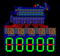
The decimal display node displays unsigned 16-bit integers. It uses the double-dabble algorithm to convert incoming binary numbers to BCD, then sends the BCD digits into some lookup tables for display. Since the algorithm expects numbers in big-endian, but the processor uses little-endian numbers, the numbers are copied to a temporary shift register to be reversed. The IO ports used are modified to access the other port's write buffer without actually performing a read operation.