01. General Description
This section describes the general characteristics of the Multi Output card.
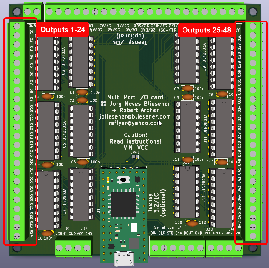
The Multi output card provides 48 digital outputs on screw terminal blocks by shifting a serial signal through six 8-bit shift registers. Additional output drivers amplify the signal and can sink up to 500 milliamperes at up to 50 volts. The serial signal can be created on board by an optional Teensy microcontroller or fed in externally. The card can be daisy-chained to provide any number of digital outputs.
The Multi output card can not drive AC (alternating current) loads, neither low nor high voltage. Do not try to connect its terminals to an AC power source or even to a wall outlet.
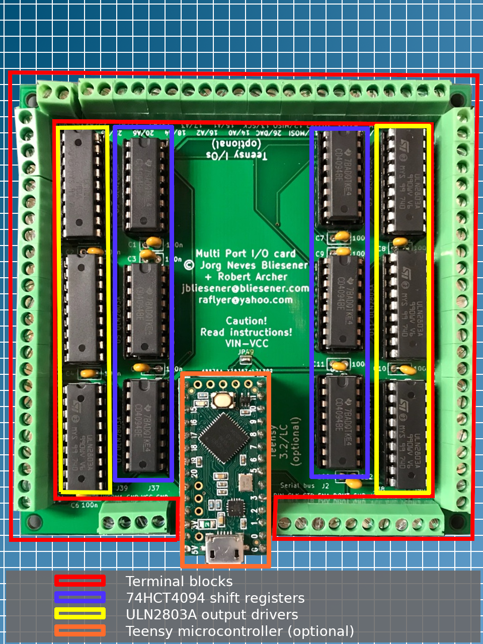
The heart of the Multi Output card are six shift registers that transform the signals sent over three data lines from your microcontroller into a total of 48 output lines. And if that's not enough, you can chain the card and add even more outputs.
Sparkfun has a video Tutorial here that explains what shift registers are and how to use the type of shift register we put on our board.
Instead of the 74HCT595 shown in the video, we're using a 74HCT4094. The only reason is that the 74HCT595 is no longer available in a DIP housing that allows you to hand-solder the card. Important: The card will NOT work with the 74HCT595. Apart from a completely different pinout, there are two subtle functional differences between the two chips that you may want to consider when you're trying to match your code and wiring with pre-existing code for the 74HCT595:
- The 74HCT4094 uses a
HIGHsignal on theENApin to activate the outputs, while the 74HCT595 uses aLOWsignal on the/OEpin for the same purpose. Make sure to set or wire the signal accordingly. To always have the outputs enabled, connect theENApin toVCC - The other, more subtle difference is the meaning of the
STBsignal in comparison to the 74HCT595'sSTCPsignal. The 74HCT595 transfers the data from the shift register to the output register only on the rising edge of theSTCPsignal. The 74HCT4094 allows to leave theSTBsignal onHIGHlevel and then transparently passes the flowing bits from the shift register to the output register while they're being shifted. If you use the FlightSimOutput library, you don't need to worry about this detail.
Another Tutorial on electronics-tutorials.ws goes a bit deeper and explains various other types of shift registers. If you don't know what D-type Flip Flops are, you may want to start on the first page of the tutorial, that explains the basics of serial data processing. And, just for the records: we're using a SIPO (Serial In Parallel Out) shift register on our card.
While the shift register performs the work of transforming a serial data stream into up to 48 parallel output lines, these don't have the power you require to drive lamps, relays, motors or other stuff. Therefore, the card also provides six ULN2803A chips that are responsible for amplifying the signal and dealing with higher voltages.
The ULN2803A chip is an open collector driver that connects an input pin to GND when activated. This is called low side switching and it has some advantages, such as being independent from the voltage you are switching.
This video explains how to use the almost identical ULN2003A chip. The only difference is that the ULN2003A only provides seven outputs, while the ULN2803A has eight outputs and a different pin numbering. Everything else shown in the video applies as well.
For those that want to understand even more details of this driver chip, there's another video here that explains the inner workings and limitations.
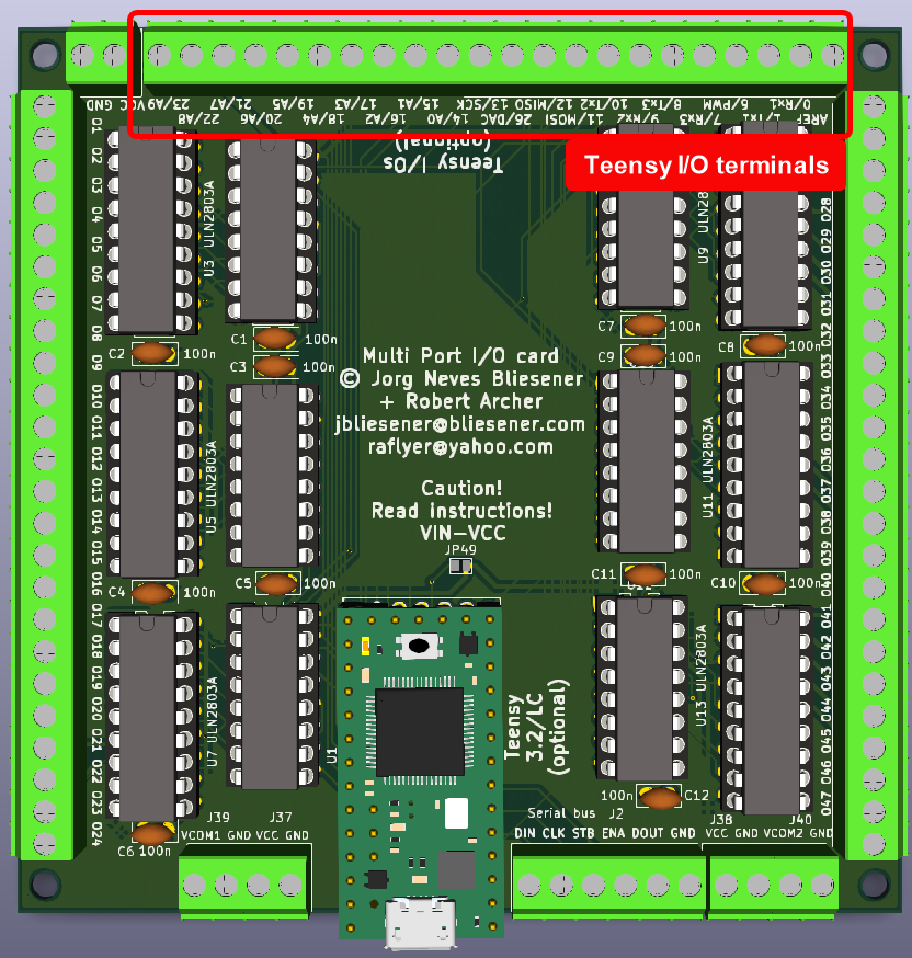
The input signals for the card can be fed externally through the data input lines or generated on-board with a Teensy Microcontroller. If you want to use the card with, let's say, an Arduino or a Raspberry Pi, there's no need to put the Teensy on board.
However, the Teensy has a series of advantages, like its native USB port that permits direct communication with X-Plane. It is programmed with the same language and environment as the popular Arduino chips and you can buy it and download all required (free) software at http://www.pjrc.com.
The board can host either a Teensy 3.2 or a Teensy LC and only uses four of its many input and outputs. Most of the remaining input and output lines of the Teensy are available on screw terminals and you can use them with your own sketches without the need for a separate breadboard.
The FlightSimOutputs library runs with Arduino as well as with the Teensy, but it provides some specific extensions for the Teensy that make it even easier to interface to X-Plane. Furthermore, you can connect up to 1024 switches and buttons to the Teensy with the FlightSimSwitches library.
The card has the following external connectors:
The 48 output lines O1 to O48 are available on the left and the right side of the card. Depending on the Output configuration these output lines are either digital TTL outputs (5 volts push-pull, up to 25 milliamperes each) or open collector data sinks for up to 50 volts at up to 500 milliamperes (not more than 2.5 amperes in total for each group of 8 output lines).
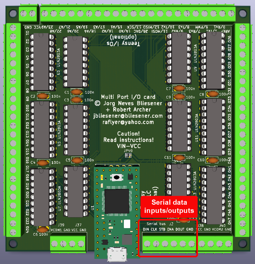
The six data inputs/outputs can either receive a serial data stream from an external microcontroller (Arduino, Raspberry Pi, ...) or provide this data to additional, daisy-chained cards.
The DIN terminal is the serial input data that is passed through all shift registers on the board. The output signal from the last shift register is available at the DOUT terminal that can be connected to the DIN pin of an additional daisy-chained card.
CLK and STB are the shift clock and the latch strobe, respectively. CLK is pulsed once for each new bit on the DIN line. After all bits have been fed to the shift register chain, a pulse on the STB line transfers the data to the output latches of the shift registers.
As mentioned before, you would probably not want leave STB on HIGH level while shifting the bits, as this would cause changes to the output signals while the data is shifted through.
The ENA line enables the shift register outputs when set to HIGH. Note that this is different from the common 74HCT595 shift registers that use a LOW signal to enable their outputs. In the standard output configuration, (with ULN2803A output drivers populated on the board), the ENA line must always be HIGH to avoid floating signals on the driver inputs, so it's actually a good practice to tie it to HIGH permanently.
The board provides a number of power connectors that receive or supply power to internal and external components. Make sure to read the section about powering the board to understand the options and implications of how to provide internal and external power.
GND is the common ground connector for both the externally switched voltage, the digital input signal and for all components on board. All GND pins are tied together.
VCC is the 5 volts supply voltage for the card's shift registers. It should not be used to power the Teensy or Arduino, but there's a notable exception for advanced users. A wrong connection on this power pin can damage the whole board, including the Teensy and a PC connected through USB.
VCOM1 and VCOM2 are the flyback (or freewheeling) diodes of the ULN2803A chips, as explained in the two videos mentioned in the ULN2803 section of this page. VCOM1 is used for output lines 1-24, VCOM2 is used for output lines 25-48.
The VIN-VCC solder jumper is used only when a Teensy microcontroller is mounted on the card. It can provide power from the Teensy to the shift registers. Please read and understand the powering section of this Wiki to understand how to use it.
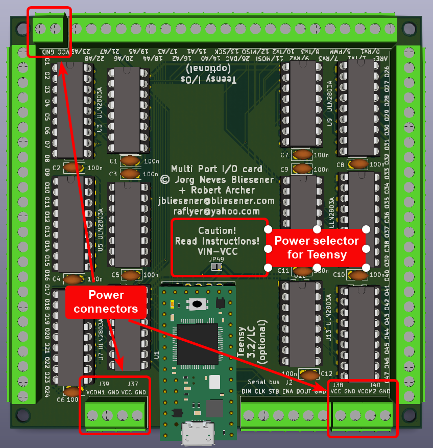
The 22 terminals on the upper side of the board are populated only if you decide to use the board with an internal Teensy microcontroller. These pins provide analog and digital input and output signals that you can use freely in a Teensy sketch.