This repository consists of circuit design details of 1 bit Full adder using 13 transistors and its simulation results. The design was implemented in Synopsys Custom Compiler tool using 28nm CMOS technology PDK.
TABLE OF CONTENTS
-
ABSTRACT
-
CIRCUIT DESCRIPTION
-
TOOLS USED
-
CIRCUIT DESIGN
-
CIRCUIT ANALYSIS
a. Transient Analysis
b. Power Calculation
c. Propagation delay calculation
-
Netlist
-
Author
-
Acknowledgements
-
References
Adders are an integral part of computational circuits like ALU in processors. This work proposes a 1 bit full adder using hybrid design style incorporating CMOS, Complimentary pass logic (CPL) and transmission gate. The 13 transistor full adder design takes 3 inputs and generates its sum and carry as output. Design is done using Synopsys custom compiler tool using 28nm CMOS technology PDK.
Full adder takes 3 inputs (A,B Cin) and generates Sum and Carry (Cout) as described in truth table below.

Fig 1. Truth Table
The Boolean expression for sum and Carry is as below :
Sum=A⊗B⊗C (1)
Cout=AB+BC+AC (2)
The circuit consists of 3 stages – A 3 transistor XNOR logic and sum and carry generation logic.
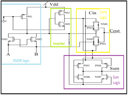
Fig 2. Circuit Diagram [1]
Transistor PM1 in XNOR logic acts as a pass transistor to supply voltage to NM1,NM2 which forms the XNOR logic. From the truth table it can be seen that the value of carry Cout is dependent on the state of the input itself. If A=B, Cout = B If A ≠B, Cout = Cin
Equality of A and B can be checked by XNOR gate as it gives a logic high when both inputs connected to it are same. A transmission gate consists of a PMOS and NMOS transistor connected in parallel. Control signal connected to the gate of PMOS transistor is the inverted signal of gate of NMOS transistor. When 2 transmission gates are connected in parallel it forms a multiplexer gate. Parallel connected transmission gate having control signal as XNOR logic output can be used to realise the Cout function.
In a similar manner the sum logic is derived from the input without depending on the Cout output signal. Output of the XNOR connected to inverter gives the XOR logic. 2 transmission gate pairs connected together with control inputs as XOR and XNOR respectively is used to give sum output. The output sum logic depends on XOR or XNOR of the inputs A,B. If A=B, XNOR logic output is 1, lower transmission gate is ON and Sum = Cin. A ≠B, XNOR logic is 0 and transistor PM5,PM6,NM6,NM7 form the second stage of the XNOR circuit to generate the sum output(Equation 1).
The proposed circuit has smaller area as lesser number of transistors is used in comparison to implementing Sum and Carry Boolean expressions using CMOS logic. As there are only 2 stages in critical path it responds faster to input signal. The design is able to generate full voltage swing at the output avoiding threshold voltage loss due to pass transistor logic.
Synopsys Custom Compiler tool was used to develop the schematic of the circuit. Simulation of the circuit was done using PrimeSim.
The schematic of the circuit is shown below
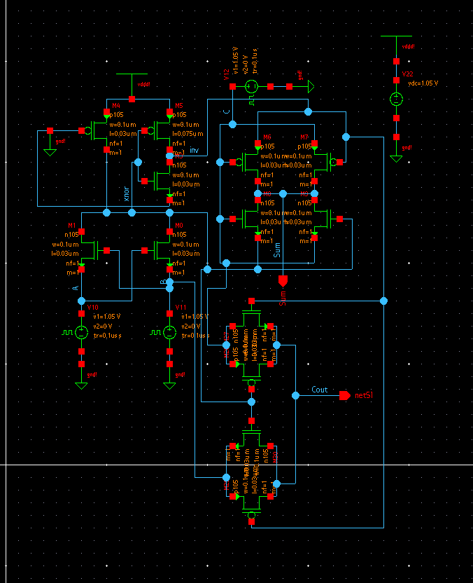
Transistor M5 used to implement inverter has W= 0.1um and L=0.075um and all the other transistors have W=0.1um and L=0.030um
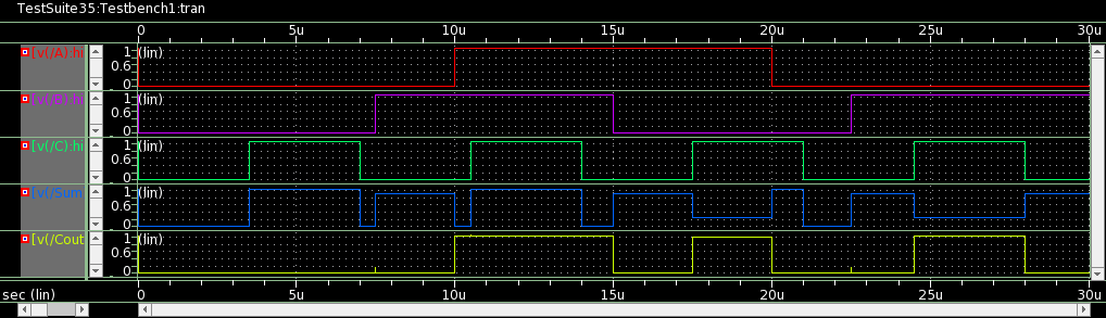
a. Transient Analysis
Transient analysis is used to observe circuit behaviour over a period of time. The 3 inputs of adder circuit A,B,C were given pulses with different period and observed the values of Sum and carry as shown below :
b. Power Calculation
Observed the current through all the sources present in the circuit A,B,C and power supply. Calculated the average value of the current using the 'measure' utility of the waveviewer.
Average current = 6.315uA
Vdd = 1.05V
Total Power = V*I = 6.63uW
c. Propagation Delay Calculation
The propagation delay of a circuit is the time taken for the output to change when the input has changed. It is calculated at a threshold of 50% of signal level at both input and output. Propagation delay is calculated for the highest delay critical path in the circuit.
The output load taken is 10fF and input slew is 0.1ns for the calculation of propagation delay. Sample Values are :

Observed propagation delay for Sum : 1.3ns
Observed propagation delay for Carry : 1.2ns
Netlist for the circuit is shared here.
Jessita Joseph, Centre for Development of Advanced Computing (CDAC), Trivandrum
I would like to extend my gratitude to Kunal Ghosh Co – Founder VSD Corp. Pvt Ltd, Staff of IIT Hyderabad and coordinators of analog design hackathon for all the support rendered to complete this design. I am immensely grateful to Synopsys India for providing Synopsys tools to develop this design.
- C. P. Kadu and M. Sharma, "Area-Improved High-Speed Hybrid 1-bit Full Adder Circuit Using 3T-XNOR Gate," 2017 International Conference on Computing, Communication, Control and Automation (ICCUBEA), 2017, pp. 1-5, doi: 10.1109/ICCUBEA.2017.8463827.
- P. Bhattacharyya, B. Kundu, S. Ghosh, V. Kumar and A. Dandapat, "Performance Analysis of a Low-Power High-Speed Hybrid 1-bit Full Adder Circuit," in IEEE Transactions on Very Large Scale Integration (VLSI) Systems, vol. 23, no. 10, pp. 2001-2008, Oct. 2015, doi: 10.1109/TVLSI.2014.2357057.
- A. K. Yadav, B. P. Shrivatava and A. K. Dadoriya, "Low power high speed 1-bit full adder circuit design at 45nm CMOS technology," 2017