My latest ZX81 clone without ULA built from discrete pin through hole components It features a PCB with the exact same size as a normal ZX81, (142 x 100mm) and features drill holes and connectors at the same locations (with the 3.5mm power jack replaced with a modern Type B USB power jack, so you can power this ZX81 clone with a simple USB power supply), and with the RF output modulator replaced with a composite video output connector, that produces a video signal that modern composite monitors should be able to accept (yes with a real front porch signal, so it works on modern TV's as well). There is no ULA needed for this clone, as all the ULA logic is replicated with modern DIP compatible logic IC's. The software (ZX-81 BASIC) fits into a cheap OTP (one time programmable) 27C256 ROM, and the bit-for bit same code as a real ZX-81 code can be programmed into a 27C256 OTP ROM, and will work exactly the same as a real ZX-81. but with a few jumper changes you can also use an original 8K ZX81 ROM. The use of a 4K ZX80 ROM is also supported. Its also possible to fit several (different) code images into the 32K ROM, and it is possible to add switches to select one image to boot with. Note that you should fill up the ROM with as many copies of the 8K BASIC ROM as will fit, meaning for a 27C256 (a 32 K byte ROM) you should fill it with four copies, and a W27C512 (64K Byte) with eight copies. Extra logic was added to simulate the same cassette loading screen patterns as a real ZX81 has. The cassette loading input logic has been eenhanced to give perfect cassette loading behaviour, even whith cassette signals generated with a laptop, for easy cassette loading. The ULA replacement logic is perfect enough to enable the use of games which use various enhanced highres graphics techniques to work flawlessly. In fact the ZX81+38 clone is easy to build, and a joy to use.
Warning: The revision 1.4 version of my ZX-81+38 contains some errors, and will NOT work as is. The main reason being that the WAIT generator flip/flop idea doesn't work, and must be replaced with a working wait circuit. As revision 1.4 is not working, and has now been replaced by revision 1,5, I have deleted revision 1,4
ZX81+38rev1,5.zip contains all gerber and drill files for the working updated and layout checked files to produce a revision 1,5 version PCB.
The file ZX81+38rev1,5.pdf is the schematic of the corrected revision 1.5 (in black and white) The only difference with rev 1.6 is that a8 is used for the keyboard connection instead of A8'
We found one more error, that I have fixed in revision 1,6: the keyboard matrix is connected to eight Address lines, A8 to A15, but the error is that for A8 a version is used that comes from the signal line passing through a 10K resistor (R1) so it is signal A8' , that is not correct, the keyboard needs unattenuated signals, so A8, not A8'. otherwise the resulting dataline does not go low enough to reliably register as "low". (actualy this was not essential, as long as the RP1 pullups are not too strong, so I changed them to 10K instad of 4K7.
Revision 1.7 fixes some small errors, and revision 1.8 has the fault fixed that lead to a mix of logic families, now only HC logic is used (in theory you can also use all LS logic, or all HCT logic, all LS logic is confirmed to work.
Because of covid (closing my Makerspace) I have not been able to build my own copy of the ZX81plus38, but I'm several people have built it and reported that revision 1.6 is working well. You can read much more about the development of my designs in my makerspace at www.revspace.nl look up my projects in the projects gallery. For example this project can be found here: https://revspace.nl/ZX81plus38_simple_to_build_ZX-81_clone for writing back you can mail me at mahjongg at xs4all.nl replace the at for the commercial at sign @, or you can use the forum of the raspberry PI organisation where I wrote about this clone in the "offtopic" section.
And I will upload kiCad files after I know revision 1.6 is working well, which can happen only if revspace reopens, and I have built and tested my own copy, and I have recovered enough from my current bad condition of what I think of as my "long-covid", only I don't remeber ever having a case of covid, but I do suffer from the same symptoms. I'm 66 now (2021/2022) so I don't see myself getting a job anymore, and consider myself retired.
I noticed that somehow I hadn't uploaded a BOM, so I added the Bill of material file in the form of and .ODS (open officie spreadsheet) file The BOM contains exact component designators for all components used from either farnell or mouser, so you will know EXACTLY which components to buy. Use version 1.8 so that you don't use a mix of logic families.
Note that R21 (the series resistor for a power LED) is NOT in this BOM, as I added it after I created the BOM, but should be 330 Ohm (if you add a Power LED) That is if you built the keyboard I designed for the ZX81plus35 that also works with this ZX81plus38, in the schematic a value of 100Ohm is used, which is also okay, although much brighter.
on june 15, 2022 I uploaded a BOM for revision 1.7 of the ZX81+38 creating some corrections R20 should be 680R, R21 should be 330 R R29 should be 1M RP22 can be 10Kx8 but 22Kx8 works better with some keyboards, C7 should be 47nF, most importantly U21 should be a 74HC04 or 74HCU04 NOT A 74HC14! There is a strong possibility the crystal oscillator won't work when using a schmitt trigger inverter (74HC14) use a HC04 or better a HCU04.
On June 23, 2022 I finished the schematic for the latest revision 1.7 version of the ZX81+38 with several small corrections. and also updated the layout. The main correction is the rotation of the keyboard-data connector J3, so the ZX81+38 is now completely compatible with a ZX-81 keyboard foil, (I will create a specific keyboard PCB for the ZX81+35, or even a real ZX81 later on) other changes are that U21 is now a 74HC04 with R29 as an 1M resistor.
JP1 is now default jumpered for a 16K ROM space, (instead of an 8K ROM space) so its compatible with the future PSG board, awhich needs the firmware for the SD interface in a second 8K ROM section, if you don't want this (you want to use four 8K selectable ROM's) then switch over JP1.
I made the crystal footpad now compatible for a SMD crystal too, and printed several texts on the sikscreen bootom and top to help with selecting options, and improve compatibility with the BOM.
I also updated a component placement drawing for revision 1,7 and uploaded it here.
Lastly for completeness, I also uploaded the ROM dump of the real ZX-81, which you are legally allowed to burn into a ROM and use with the ZX81+38.
On 5 juli 2022 I discovered that KiCad had changed back to the logic family of some libraries for wich I had changed the original logic family from LS logic to HC logic. I intended that all logic would be HC logic, just like in my ZX84+35 initial clone. But this bug in KiCad may cause problems because HC logic and LS logic are incompatible. So the first thing I did was updating the BOM, also to see if there actually were HC replacements for the LS logic I had used by mistake. Luckily all the HC logic I needed was available in DIP. Next up will be revision 1.8 of the schematic, which will also get a clock inverter using a spare half of a flipflop. This might be necessary to solve a timing error that can occur with EPROM's that are too slow to put pixel data into the shift register, which results in all black character squares (due to the databus pullups that pull the databus high when nothing is driving it). Then I will correct the component placement diagram which also shows some wrong logic families. My last remark is that although theoretically the ZX81+38 should not work with mixed logic, it seems that in practice it still seems to work as I have reports that it does! I finished building up my own copy with mixed logic so soon I can check this for myself. Also note that I no longer recommend using sockets with machined pins, use dual wipe sockets instead. This is reflected in the BOM. Lastly perhaps this clone will not work with original N-MOS Z80 chips, its recommended to use modern (C-MOS) versions, such as the Z84C0008PEG.
on 26 July 2022, I updated the BOM (Bill of materials) for ZX81+38 revision 1.8, adding more reichelt order codes (I have ordered my own missing HC logic chips from there, as farnell is no longer an option for me). They even had all the correct connectors! Added a new component placement drawing that corrects the wrongly mixed logic family's and adds some extra info, use this drawing for revision 1.8 Addded rev 1.8 Schematic (.PDF in black and white) for other (.PNG older or color schematics) see my Revspace pages at www.revspace.nl/projects.
Uploaded PCB production files gerber and drill files, (I checked them with a gerber viewer, they should be okay) this version has all the latest improvements, inclusing clock inversion and the copper fill isolation around JP1.
To avoid confusion when downloading unsuitable older files I have removed all older (pre rev1.8) files, older schematics etc can be found on my revspace pages. if you need older gerber files contact me at mahjongg@xs4all.nl or visit the offtopic section of the raspberry PI foundation where I have pages about my projects (I'm a moderator there).
On august 4, 2022, after many request I decided to zip up my KiCad project directory for the ZX81+38, and upload it to GitHub, so you can duplicate my effort, and create your own version of the ZX81+38. Note that at this moment I still have not got my own version working, I'm still missing a 74HC74 IC, but many people have reported that they got my ZX-81 clone working, so I decided to keep my promise to completely open source my ZX-81 clone. Please if you do, don't remove my name from the PCB, and schematics! If you have any questions or remarks, you can reach me at mahjongg@xs4all.nl
by the way, if you need a manual for your ZX81+38 you can find it here: http://www.retro8bitcomputers.co.uk/Content/downloads/manuals/zx81-basic-manual.pdf
Also, if you are using a real ZX-81 keyboard foil then you need the connectors, (as you cannot solder pins to the foil) the actual connectors you need are Molex parts 22-02-3053 and 22-02-3083. Note when soldering that you solder them in with the correct orientation, as the two foil ends are metalized on diferent sides, and so the 5-pin 22-02-3053 should be mounted 180 degrees rotated compared to the orientation of the 8-pins 22-02-3083. If the orientation is wrong the connectors will not make contact with the metalized side of the foil. You can find these connectors from different distributors, or from https://www.sellmyretro.com/offer/details/set-of-molex-keyboard-membrane-connectors-for-sinclair-zx81-10859
ONE MORE SMALL REVISION WAS NEEDED REVISION 1.9
When testing the joystick interface we found out that it wasn't working, R23 should be 1 K not 10K, and I forgot to add five pulldown to GND resistors on the bases of the five 2N3904 transistor, the latter means a large layout change, I opted for a 6-pin resistor (star) network with 5 10K resistors, and I placed it between the SRAM chip and the 5 2N3904 Transistors, note that pin 1 (the common pin) is located on top). I remade all the files anew for revision 1.9 and replaced the existing files with revision 1.9 files here. The .ZIP file with the KiCad files now only contains the three necessary files: that is: ZX81plus38.kicad_pcb ZX81plus38.kicad_pro and ZX81plus38.kicad_sch
As it turned out that CO2 and CO3 had a misleading schematic symbol, that caused me to use the wrong pin, as it was the signals were connected to the RING of the jackplug, not the TIP,(Of the Tip/Ring/Sleeve or TRS connecvtions) so I corrected that so now audio comes out, and goes into, onto the TIP connection (as is normal for mono audio), also I corrected values for C7, C8, and R59, and these corrections are in the new schematic, the BOM and the component overview drawing, all corrected files were replaced even the KiCad files.
On October 6, 2022 I uploaded a new BOM, some small errors were repaired, the 74HC11 from mouser was listed as a 74LS11, and the SRAM from mouser was a "skinny dip" version instead of a regular 600mil DIP.
You can watch a youtube explaining the build of the ZX81+38 here: https://www.youtube.com/watch?v=6a8wxj9vJjU it explains ordering the PCB's assembling the PCB's programming the ROM, and testing the computer. Note that for a cost analysis you often have to give the dimensions of the PCB, for the ZX81+38 PCB it is 142mm wide and 100mm high. for the keyboard PCB it is 158mm wide and 64mm high. But don't worry these dimensions are only used for a price assemment, the actual dimensions of the PCB's are derived from the gerber files. The main PCB is a two layer one, but the keyboard in priciple is only one layer, but if one layer PCB's are not supported choose two layers, the manufacturor will actually only create the top layer.
REVISION 1.10 ONLY FIXES THE LOCATIONS OF SOME MOUNTING HOLES, ELECTRICALLY IT IS THE SAME AS REV 1.9
For a keyboard with real buttons. on September 8, 2022. I finished my keyboard PCB, revision 1.1. I uploaded the schematic, the PCB production files, a Bill of material specifically for the keyboard, and a keyboard overlay (.PDF) which you can print out, laminate with transparent plastic, punch holes for the 40 keyboard plungers, and glued on top of the buttons. and a Bill of material for the keyboard with 40 keys a power LED, and solder pads for three flatcables, that are prepared so that they have wire ends with 2.54 pitch (every other wire with an 1.27mm pitch is not used) three flexcables are used with 5-wires 3-wires (for the LED) and 8-wires). revision 1.2 was made because there were some errors in the lettering below the keys, now the text "T Y U I O P" is corrected and the "10" was changed to "0", also the lettering was made a bit bolder. This change only pertains to the silk screen, nothing else has changed. so you can use the revision 1.1 BOM. and I updated the KiCad files. If you already made a revision 1.1 PCB, no worries, the lettering is not needed when you use the keyboard overlay, and nothing else has changed. The copper text on the keyboard now reads 1.2. Note that when ordering the PCB you often have to give PCB dimensions for cost assesment, for the keyboard the dimensions (as said above) are 158mm wide and 64mm high. This is a SINGLE SIDED PCB, so there is NO bottom copper! I also added the keyboard overlay, which previously was only to be found on my ZX81+35 pages, you can print this out (preferably in color)plastify it wit self sticking transparant plastic, it should fit exactly over my keyboard. You can then punch 40 4mm holes in it for long button stems, or use low profile, low travel keys and simply glue the overlay over the buttons and press on the buttons through the plastified paper.
I have also designed a very simple variant of the TZXDuino, an Arduino nano based playback device that can convert a .TZX file for a sinclair spectrum, or ZX-81 from a SD-Card to an audio signal that can be used to load a cassette file (game) into a sinclair computer, you can find it as the TZXDuino Pico project on the mahjongg2 github pages. I plan to use it to test the cassete interface of my ZX81+38 clone. The PCB is very small only 37.1 mm wide, and 47.2 mm high and it is a 2 layer board.
from various sources I heard that EPROM's (OTP's) are almost unobtainable. I have done a bit of research, and yes, it seems OTP ROM's are very hard to get, due to the chip crisis. I found however one option that will work, you can buy an 28C64 for about ten euro. from Reichelt its an 8K x 8 reprogrammable (EEPROM), you can buy it from here: https://www.reichelt.nl/nl/nl/eeprom-64-kb-8-k-x-8-5-v-150-ns-pdip-28-28c64-150-p1946.html?&trstct=pol_2&nbc=1
And yes, you need to change a wire bridge, as the 28C64 has a different pinout than a 27C64 but that isn't a very big deal.
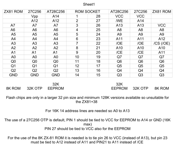
You can find a diagram showing the differences between a 27C256 and an 28C256 here, also showing the pinout of the original ZX-81 ROM: https://revspace.nl/images/thumb/6/68/Rom_pinouts_for_ZX81%2B38_resized.png/707px-Rom_pinouts_for_ZX81%2B38_resized.png
For a 28C64 the only real difference is that pin 27 must be tied high so that /WR is inactive, so switch jp10 to tie pin 27 high, not low.
It is expected that 27C256's will become available beginning next year (2023). Note that due to the fact that an 28C64 is a small EEPROM, it only contains 8K, so don't buy it when you plan to later add the planned PSG expansion board, as this needs another 8K firmware (although a normal ZX-81 also doesn't have an option to simply add extra firmware, but there will be an extra 8K ROM space on the PSG board).
Note that if you own a (broken) ZX-81 you can use its ROM but there are some more jumpers to change, note the ROM pinout diagram above.
Another solution is to buy a new old stock EPROM , the ones with a glass windows form a Chinese reseller these have the exact same pinout as modern OTP's as OTP's simply contain the same DIE (chip) as UV erasable EPROM's, so they have the exact same pinouts as OTP's.
As of April 2023 it seems that 27C256 EPROM's are again in stock!
There are several places where you can read the original ZX-81 manual online, one of those locations is here: http://otremolet.free.fr/otnet/otzx/zx81/basic-progr/
To order PCB's (from PCBWay for example) download the "production files" map of the PCB you want, the downloaded map will contain all the files you will need, that is both gerber and drill files, but most often the PCB manufacturer will want all these files in a single .ZIP file, so you have to zip up all the files in the map into a single.ZIP file first. Also most PCB manufacturors will want to know the dimensions of the PCB so they can make a price assesment these are the sizes you can quote:
The ZX81+38 PCB is 142.2 wide and 99.1 mm high and dual sided, although the PCB has an edge connector the original ZX-81 PCB's edge connector was neither bevelled nor gold plated, so I would ignore gold plating the edge connector, as creating one makes the PCB considerably more expensive.
The keyboard PCB is single sided with copper and silkscreen on TOP! the PCB manufacturor will see that it is a single sided PCB as gerber files for the bottom side are not included, and there is text on the top side, but if there is an option to write a message it can't harm to mention these facts to the PCB manufacturor.
If you also want to create my TZXDuino PCB, (a device that can read files from an SD-card and outputs cassette loading audio) then note that it is a simple dual sided PCB that is 47.2mm high by 37.1mm wide. Its in my TZXDuino-Pico repository. It is actually meant to be built into a ZX-Spectrum, but can work with ZX-81 .TZX files. Note that its a simplified form, original TZXDuino kits are also available from several vendors.
when filling in the order detail, you should use the suggested default, like a thickness of 1.6mm, but you can order a different PCB color than the default green, but keep an eye on the price, as some options come with a price!
If you order PCB's from China (PCBWay) then to pay for them there are numerous options, but if you don't have PayPal, or a credit card it might be that your only option is to order via Aliexpres, and that way is a bit strange. Simply set they paymethod, and the mailing option to aliexpress, and order, note down the price, then you will be transfered to aliexpress to a web-page where your PCBSeller has a sellers page. but note that instead of the noted down price, they quote a very low price, normally one dollar. Now they will give you the option to buy more than one item, increase the numbers of items you want to buy untill the price for your order is the same as the price the PCB manufacturor asks for, so say the PCB manufacturer asks for euro 47.50 then increase the number to 48, so the price becomes euro 48 then continue to order.
there are 3D designs available to 3D print a zx-81 case, or you can use a real ZX-81 case from a defective ZX-81. Another possibility is to design a wooden case, either from thicker wood, or from 4mm thick plywood (laser) cut and glued together, or as one user did make one from LEGO! you can download a lEGO design from here: https://rebrickable.com/mocs/MOC-129979/akilling/lego-case-for-zx81-plus-38/#details
The canonical ZX81 hardware/software hobby designer Wilf Rigter designed a highresolution system for the ZX-81 in 1986 and wrote about it here: https://archive.org/details/zx-appeal/ZX-Appeal%20Jan%2086/page/12/mode/2up?view=theater (I looked in later issues but found no other information about WRX16). in this article he stated that for it to work a ZX-81 needed an extra 8K RAM pack at 8K to 16K, (the 8K following the ROM) and a Z80 that supported 8-bit refresh! Most Z80's at the time only supported 7-bit refresh counters (7-refresh address lines) but it seems you could buy Z80's that supported 8-bit refresh in 1986. I found out that the Z84C0008PEG does have an 8-bit refresh counter though.
The ZX81+38 (when wired for 8K ROMS space) does have RAM at 8 to 16K, but in this case that RAM is a copy of RAM that is duplicated elesewhere, in any case it seems that currently revion 1.9 of my ZX81+38 does not supports wilf rigters WRX16 high resolution solution. And trying to use a game based on WRX16 currently crashes, there are a dozen or so programs including a few games that use WRX16. you can find a list here: http://www.pictureviewerpro.com/hosting/zx81/fredn.htm
But please note that most other (pseudo) high resolution games that work on an unmodified ZX-81 do work, examples are manic Miner for the ZX-81, and many others, just a few examples; Against the Elements, JB Racing, Starflight 2002 and the Rezzurection demo are shown here working https://www.youtube.com/@ManfMoser
My current conclusion is that an unmodified WRX16 won't work as is, but note that with a small re-write of the WRX16 code, so that it uses the extra 16K RAM instead of an 8K RAM board, it should work. (see the issues section) I tried to contact Wilf, but so far he has not reacted to my e-mail.
If you have a ZX81+38 revision 1.9 PCB you will notice that it uses a SMT version of the 13MHz crystal. If you cannot find a SMT version (recognizable by the plastic carrier underneath it and flat pins bent sideways) then it is possible to use a pin through hole crystal, simply use a piece of paper and stick it over the wires, punching the wires throug the paper, then bending the wires outward, and cutting the wires off a few mm beyond the metal of the crystal. The paper isolates the pins from the metal base of the crystal. then solder the wires to the metal pads.
I uploaded new versions of the component overview drawing and the ZX81+38 BOM. The drawing has the position of the crystal, and the 15pF capacitors corrected, and the Value of RP1 corrected from 1K to 10K. 1K probably works, (with revision 1.9 PCB's that use A8 not A8' but both the schematic the BOM uses 10K, as does the original ZX-81. The BOM only has the correction that the 3.5mm jacks are not CLIFF FT6320 (that is the wrong model), but the cheaper FC68131, that doesn't have switches and has the correct pin arrangement. By the way the BOM is in the open source open office .ODS format, which can be opened with the free open office software, or an online tool.and probably also with Microsofts spreadsheet tool if you choose to open a .ODS file with it. I prefer open source formats..
I wrote a document explaining the build process of the ZX81+38. For inexperienced hobbyist note that building the ZX81+38 is NOT a simple affair, you need to have experience in soldering. Also I explain the process of finding the fault if your ZX81+38 doesn't work at first try. Please read the "building and testing the ZX81+38" document. If you have any questions or remarks, you can reach me at mahjongg@xs4all.nl Also I might, for a fee, program (and test) a 27C256 EPROM for you, if you do not own an EPROM programmer. Please contact me at my e-mail address.
I wrote a small document about the use of jumpers on the zx81+38, what they do, where they are on the board etc. But note that normally you don't have to change a single jumper, they are all pre-set with a small wirelink, you must cut to change the setting. This document is just for the more curious people, or for those who do not want to use a 27C256, perhaps because they want to use the original zx-81 ROM, or they want to invert the video signal from a white background to a black background.
I'm writing this as this information is hard to find elsewhere.
The ZX81 memory map is divided into four 16K parts.
The first (lower) 16K part, contains the ROM (as it’s only 8K, you would normally get a echo of the first 8K in the second 8K, but the 27C256 contains 32K, so you can put something else there). this ROM-space is normally set to 16K default, so you can use the second 8K for ROM expansions, such as the SD-Card reader firmware on the (PSG) sound + SD-card expansion board that I'm planning to design. but you can force the ROM-space with a jumper to be only 8K, and then the second 8K becomes RAM.
The second 16K part, is the normal RAM area. On a normal ZX-81 with 1K RAM this space contains 16 copies of the 1K RAM space.The firmware detects these are copies.
The third 16K of a real ZX-81 will have more copies of the ROM, but the ZX-81+38 will not, but have copies of the RAM instead, as ROM space is limited to the first 16K.
The fourth and last 16K, is more echoes of the RAM. However, it’s important to note that the hardware detects this, and uses it for the video generation logic.
Revision 1.10 is electrically the same as revision 1.9, the only changes are that the exact location of a few non plated holes were moved to a more correct location, so that the PCB will now completely fit into the enclosure of a real ZX-81. Revision 1.10 should be the final version. I have uploaded the KiCad files for version 1.10 of ZX81+38. I also updated the component placement drawing with R29 as 1M and C1 and C2 as 4.7pF (like the BOM) The BOM of revision 1.10 has a small correction farnells order code for RP1 is now for a 10K resistor pack instead of the wrong 4K7 resistor pack.
The only difference with the ZX-81 hardware wise that for PCB needs to be fixed is that the RF modulator of the TS1000 is different, and has the RCA output on the other end of the modulator, so the enclosure of the TS1000 has the hole for the modulator near the back of the enclosure instead of next to the other connectors. Other changes were that the TS1000 had 2K or RAM, and a 60Hz refresh rate, but because the ZX81+38 already has 16K (32K if enabled) and has a jumper for 50 or 60Hz refres, no other hardware changes are needed.I had a look at the layout, and it seems possible to move the crystal and the 74HC04 down to make place for the RCA connector. This version will get its own project, named TS1000plus41.
I was told that a Facebook poster in the ZX-81 owners group claimed he found an error in the component placement drawing, after investigation I found not one, but two errors! The creating of this drawing is a completely manual process, so human errors can occur, and in fact the drawing has been repaired several times. This latest drawing now show that the resistor that is R59 and was labelled 47K was in fact 10K, and the resistor R56 that was labelled 10K was in fact 47K. So I wisakenly swapped the two resistor values, because I mis-identified them while creating the drawing. These two errors change the levels of the output voltage and input voltage (needed) for the cassette input and output levels, so if you have difficulty with loading or saving please check you have placed the right resistor values for R59 and R56. The component placement drawing is now correct (March 17, 2024) the values in the schematic, and BOM remain correct. I'm now a member of the ZX-81 owners facebook group, so you can ask me questions there!
This BOM has multiple suppliers, so improve the chance of finding a part you need. Created because a builder complained he could not find a part anywhere, so I added two more suppliers next to farnell, namely mouser and reichelt. It can also be used to compare the same part from to suppliers, so you can order his part from any other supplier. The new BOM is called "EXTENDED ZX81plus38_BOM_with multiple suppliers revision 1.10.ods" it can be opened with the free and open source spreadsheet open office, or any other spreadsheet that can handle .ods spreadsheet. Another reason to compare suppliers is to find the best prize. If you are American, you might want to buy from Digikey, there is another BOM created by a builder (so not by me) with digikey parts in the "issues" section, issue #18.
I joined facebook as Martin de Jong, so I can answer questions about my ZX-81 clones in among other groups the "ZX-81 Owners Club". see uou there! I'm also on various ZX-81 fora, like forum.tlienhard.com as mahjongg.