STM8 EEPROM unlocking bug
I just found a hardware bug in STM8 CPU which cause instability of EEPROM write operations. For those who wander around looking for clues, I hope you will find the answer here.
You try enabling write access to the EEPROM on STM8 microcontrollers and carefully follow the instructions in the reference manual from STMicroelectronics. However, you can't reliably get the result you want. Sometimes it works sometimes it doesn't.
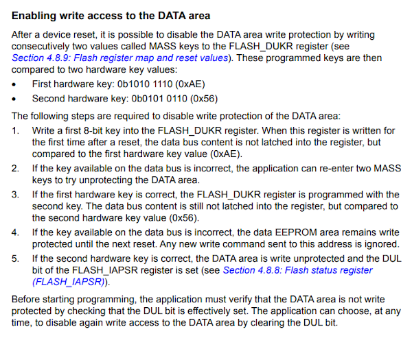
You read the reference manual from STMicroelectronics which looks like this:
And come up with what majority of people would
like Mark Stevens
if (FLASH_IAPSR_DUL == 0) {
FLASH_DUKR = 0xae;
FLASH_DUKR = 0x56;
}

// write to EEPROM

FLASH_IAPSR_DUL = 0;
or the standard peripheral driver released by STMicroelectronics themselves
void FLASH_Unlock(FLASH_MemType_TypeDef FLASH_MemType)
{
  /* Check parameter */
  assert_param(IS_MEMORY_TYPE_OK(FLASH_MemType));

  /* Unlock program memory */
  if(FLASH_MemType == FLASH_MEMTYPE_PROG)
  {
    FLASH->PUKR = FLASH_RASS_KEY1;
    FLASH->PUKR = FLASH_RASS_KEY2;
  }
  /* Unlock data memory */
  else
  {
    FLASH->DUKR = FLASH_RASS_KEY2; /* Warning: keys are reversed on data memory !!! */
    FLASH->DUKR = FLASH_RASS_KEY1;
  }
}
but nothing works reliably.
It might work sometimes but not always.
You google for the solutions and ends up here.
Perhaps, I got more luck than you people because the hardware faults in my application can reveal some info of the failure. I am storing counting value in the EEPROM. My code is not that much different from Mark Stevens', but since I am storing counting value, I immediately notice that for some reasons only even value has been saved to the EEPROM. This behavior also matched with what Mark Stevens reported. However, in my case, unlike Mark Stephens', I can be sure that the failure is not random.
If you want to see what I see or testing out my software on your hardware you can grab the code with build instructions from this branch.
Anyone seeing the result would immediately conclude that the order of key is wrong.
Our KEY1 is CPU's KEY2, and our KEY2 is CPU's KEY1.
Our perspective | CPU perspective
----------------+----------------------------------
Send KEY1       | Receive KEY2, Do nothing
Send KEY2       | Receive KEY1, Do nothing
Write           | Do nothing
Lock            | Do nothing
Send KEY1       | Receive KEY2, Unlock EEPROM write
Send KEY2       | Receive KEY1, Do nothing
Write           | Write to EEPROM
Lock            | Restrict EEPROM write
This is why I got only even numbers in the EEPROM.
Once concluded I unreverse the key so the MASS keys sequence would effectively be the same for both program memory and data memory.
FLASH->DUKR = FLASH_RASS_KEY2; /* Warning: keys are reversed on data memory !!! */
FLASH->DUKR = FLASH_RASS_KEY1;
become
FLASH->DUKR = FLASH_RASS_KEY1;
FLASH->DUKR = FLASH_RASS_KEY2;
And it works!!!
I can now record both odd and even numbers.
Unfortunately, I knew right away that I only just rediscovered what ST's engineers encountered years ago. There must be a good reason to make them comment something like this in their code.
FLASH->DUKR = FLASH_RASS_KEY2; /* Warning: keys are reversed on data memory !!! */
FLASH->DUKR = FLASH_RASS_KEY1;
I presume that the reversal of key order is unexpected even inside of ST. They changed and documented their "corrected" version of the key sequence everywhere.
I suspected that the good reason is that ST's engineers observed and saw the same behavior I have seen, and the solution to the problem is to reverse the order of MASS keys.
It seems that the real hardware bug here is the fact that the internal state of FLASH_DUKR register did not get reset properly. It can't merely solve by reverse the order of MASS keys. The actual issue lies beyond.
Luckily, software solutions to mitigate the bug is possible. We can exploit the fact that STM8 CPU allow trying the first byte of MASS keys for EEPROM unlocking.

Even if we don't know which bytes the FLASH_DUKR register will consider as the first byte of the unlocking sequence. We can just do
while (!(FLASH->IAPSR & FLASH_IAPSR_DUL)) {
  // the order here does not matter anymore
  FLASH->DUKR = FLASH_RASS_KEY1;
  FLASH->DUKR = FLASH_RASS_KEY2;
}
to crack the code.
There are 2 possible scenarios for the workaround code.
Either
Our perspective | CPU perspective
----------------+----------------------------------
Send KEY1       | Receive KEY1, Do nothing
Send KEY2       | Receive KEY2, Unlock EEPROM write
Write           | Write to EEPROM
Lock            | Restrict EEPROM write
or
Our perspective | CPU perspective
----------------+----------------------------------
Send KEY1       | Receive KEY2, Do nothing
Send KEY2       | Receive KEY1, Do nothing
Send KEY1       | Receive KEY2, Unlock EEPROM write
Send KEY2       | Receive KEY1, Do nothing
Write           | Write to EEPROM
Lock            | Restrict EEPROM write
we will always get the result we want.
You can grab the example workaround code with full build instructions from this branch.
And that's it. I think that is what you came here for.
After the CPU execute the workaround code for some time, the key sequence seems to be stable at the reversed order, just as described in the reference manual. I don't know how to reset it back to the ascending order state, but there is no guarantee it will never change again. So I would recommend using the workaround solution even if your microcontrollers are fine with the EEPROM now, it works regardless of the ordering.
Sarun Rattanasiri
A full stack software architect, being able to work with small devices, complex enterprise backend systems, beautiful and robust frontend, and everything in between. Proficient in both business and technical languages. Not the smartest kid in the room, not a fast learner, but one who understands.
In my free time, I like to read, sleep, and do some lite coding. I have a broad knowledge of many things. If you want to discuss just drop me an email at the same address as appeared on git commits in this repository.
- Mark Stevens (https://blog.mark-stevens.co.uk/)
- MCD Application Team of STMicroelectronics (https://www.st.com/)