VSDIAT Skywater 130nm Physical Verification, technology overview, PDK and EDA tools workshop
- Day 1 - Introduction to SkyWater SKY130
- Day 2 -DRC/LVS Theory and labs
- Day 3 - Front-end and back-end DRC
- Day 4 - Understanding PNR and physical verification
- Day 5 - Running LVS
The SkyWater Open Source PDK is a collaboration between Google and SkyWater Technology Foundry to provide a fully open source Process Design Kit and related resources, which can be used to create manufacturable designs at SkyWater’s facility. This PDK is targeting the SKY130 process node.
Open source EDA tools can be used with the Sky 130 PDK:

Libraries in the Sky 130 PDK:

This is the layer stack in the Sky 130 process. The Local Interconnect, made of TiN, is quite characteristic of this process, and is only used for very short distance interconnects on devices.

Deep N well is available for noise isolation:

There are 5 levels of metal:

Some layers are generated automatically by the Magic layout software. For example, the NPC or nitride poly cut layer, is generated automatically by Magic from the position of other layers, like the poly and the contacts.

The RDL is done separately:

Inverter in xschem and simulated with ngspice: (pre-layout)

Prelayout sim result:

This is the layout:

LVS clean:

Result of post-layout extracted sim:

Physical Verification is aimed at ensuring that we don't manufacture "very expensive glass".
It consists of a number of routines to ensure the manufactured devices will be functional and will perform as expected. As part of Physical Verification we will need to run checks such as:
- Design Rule Check (DRC)
- Layout vs Schematic (LVS)
- XOR comparison of layouts
- Antenna Checks
- Electrical Rule Checks (ERC)
- Aging, etc.
Two critical steps of Physical Verification are:
DRC (Design Rule Checks): These are required to make sure the design layout can be fabricated at the foundry without issues. LVS (Layout vs Schematic): This is key to ensure that the circuit we are sending for fabrication matches the design schematics.
Otherwise we may be manufacturing very expensive glass.
We start with a GDS of an AND2 gate standard cell, read in from the PDK standard cell GDSs available that come with the PDK from the foundry:

We played with cif istyle etc to see the effect.
Then we looked at port index number that Magic arbitrarily assigns to each pin after reading in the GDS.
For example for VPWR Magic says that the port index is 1.

But then we checked the .spice netlist for that AND2_1 gate from the PDK and we noticed the port order in the .spice netlist of it doesn’t match the order in the GDS read in by Magic.

Everything that you need to know about a cell is contained in the GDS, the spice file and the LEF file of that cell. Magic uses info from these 3 places when reading in the GDS, to make most sense of it.
We read in the LEF data for the cell in Magic: lef read /usr/local/share/pdk/sky130A/libs.ref/sky130_fd_sc_hd/lef/sky130_fd_sc_hd.lef
After reading the LEF, now Magic has the info to know the actual use and class of each port in the cell:

With this TCL script Magic can also know the right port order, from the .spice file: readspice /usr/local/share/pdk/sky130A/libs.ref/sky130_fd_sc_hd/spice/sky130_fd_sc_hd.spice
Now after running this, Magic knows the correct port order, matching the .spice file:

Abstract views:

But abstract views don’t have the transistors in them. They are more concerned with placing and routing.
Trying to write an abstract view to a GDS is not a good idea and Magic will warn you that it’s not likely a good idea.

Reading back a GDS written from a LEF will produce layers that don’t make sense.

However there is this trick where we can put in a LEF standard cell in our GDS layout, save the GDS, then reopen it, and Magic then pulls the actual layout (not abstract) for the standard cell, because it knows the path to where to find the layout from the libraries path.


To descend into the layout of a cell: select it with i and press greater than key > . If we type property inside the standard cell we have descended into, we see its an abstraction:

To return back up to the cell above, type the less than key < .
Now we try to replicate a standard cell layout like the one in the PDK, but we are going to try to build it up from the vendor GDS, annotate it with the LEF and SPICE information, and get a .mag layout that looks exactly the same as the one in Magic’s search path.
For that we do:
gds readonly true
gds rescale false
gds read /usr/local/share/pdk/sky130A/libs.ref/sky130_fd_sc_hd/gds/sky130_fd_sc_hd.gds
load sky130_fd_sc_hd__and2_1
Annotate it with LEF:
lef read /usr/local/share/pdk/sky130A/libs.ref/sky130_fd_sc_hd/lef/sky130_fd_sc_hd.lef
Annotate it with SPICE:
readspice /usr/local/share/pdk/sky130A/libs.ref/sky130_fd_sc_hd/spice/sky130_fd_sc_hd.spice
The result is:

Note the cell name above is my_sky130_fd_sc_hd__and2_1.
Comparing both layouts ensures they are both the same:
tkdiff my_sky130_fd_sc_hd__and2_1.mag /usr/local/share/pdk/sky130A/libs.ref/sky130_fd_sc_hd/mag/sky130_fd_sc_hd__and2_1.mag
Basic extraction: After running
extract all
ext2spice lvs
ext2spice
We get .ext (intermediate file) and .spice file. We can compare this extracted spice file and it’s the same as the spice subcircuit given in the PDK.
This is the spice extracted:

This is the spice in the PDK:

If we extract with C, then the parasitic caps get inserted in the netlist:
ext2spice cthresh 0
ext2spice

RC extraction (in development):
ext2sim labels on
ext2sim
We get 2 new files, .nodes and .sim:

Now we extract resistances:
extresist tolerance 10
extresist
Now we get a new file, .res.ext:

That .res.ext has the resistance info that has to be inserted into the .spice netlist.
Now we run ext2spice again and we finally get the .spice with R and C:
ext2spice lvs
ext2spice cthresh 0.01
ext2spice extresist on
est2spice
Now the .spice file has the Rs and Cs:


DRC: Script to run DRC on a layout:
usr/local/share/pdk/sky130A/libs.tech/magic/run_standard_drc.py /usr/local/share/pdk/sky130A/libs.ref/sky130_fd_sc_hd/mag/sky130_fd_sc_hd__and2_1.mag
We get the DRC result in a text file:
sky130_fd_sc_hd__and2_1_drc.txt
We see that the standard cell has DRC errors but that’s because the standard cell needs cap cells around it to close well and substrate connections.

While we are working with the layout in Magic, if we have the DRC style set to “fast” (for fast interactive DRC) then it will not check all DRCs, just some, so we may get a green DRC tickmark while doing layout, but when we run DRC with drc style set to “full” it will show all the DRCs.


If we set DRC style to full and run drc check, we will see the DRCs in Magic.

With drc why and drc find, it will highlight where the DRCs are and the reason.

Notice how if we add the cap / tap cells around the standard cell then the DRCs go away.

LVS: First of all, in /netgen directory, remember to copy the setup.tcl file!!! (how intuitive)
cp /usr/local/share/pdk/sky130A/libs.tech/netgen/sky130A_setup.tcl ./setup.tcl (unintuitive but it has to be done)
We extract a simple LVS netlist again from the layout with:
ext2spice lvs
extspice
Then we run LVS from /netgen dir:
netgen -batch lvs "../mag/my_sky130_fd_sc_hd__and2_1.spice my_sky130_fd_sc_hd__and2_1" "/usr/local/share/pdk/sky130A/libs.ref/sky130_fd_sc_hd/spice/sky130_fd_sc_hd.spice sky130_fd_sc_hd__and2_1"
Notice that we are LVS’ing against this huge schematic mega-netlist that is in this big sky130_fd_sc_hd.spice file of the PDK which contains all the netlists for all the cells, so that’s why we give it also the name of the cell in particular, sky130_fd_sc_hd__and2_1.
We get LVS clean:

XOR comparison: To test this functionality we load up our AND2 gate, we make a small mod to it (cut a small stripe of LI on the side).
Then we save it as another cell for comparison, then flatten it, call it xor_test, then reload the non-altered AND2 layout, and then run the XOR comparison of the non-altered AND2 layout against the altered AND2 layout, like this:

Then we load the result xor_test, and we see it has correctly found that the XOR difference is in the stripe that we cut out before.

A more realistic example of using the XOR test: we open our AND2 gate with the tap cell from before, and we shift the AND2 gate a tiny amount to the side, so it’s misplaced over the tap cell, almost unnoticeable, something that could happen during a chip design.

Then we XOR this versus our original AND2 gate plus tap cell. And we see that the XOR catches the difference clearly.


Skywater 130 DRC rules: https://skywater-pdk--136.org.readthedocs.build/en/136/rules.html
Local interconnect (LI) Made of TiN (titanium). Look at the resistances.

Magic has parameterized devices (like pcells in commercial tools).


Magic generates appropriate implant masks based on device type specified in Magic, but in Magic you won’t see implant masks.
But you will see device ID layers, which tell Magic what type of device you are trying to create, and then when Magic exports GDS it will create the appropriate implant masks, based on those device ID layer.

Wells and taps are important If you put down a standard cell you need to then put down somewhere an appropriate tap cell so all wells are biased correctly.


Deep N wells in Sky 130 For noise isolation mainly.


Deep N wells do take quite a lot of space and they require to be well far apart:

High Voltage rules: Use of the HVI layer

In high voltage regions, poly, diffusions etc has different spacing rules.

Mvdiff is for making high voltage devices around 3.0V and 5.0V.
There is yet another even higher voltage layer, called UHV, which is for really high voltages like 20V etc.
Resistors: You have p diffusion resistors and poly resistors. Better to stick to poly resistors whenever possible.

Most of the time in analog you will use pcell type resistors rather than custom layout resistors.
Caps: You have these types in Sky130:

Varactors: Varactors are formed like MOSFET transistors EXCEPT USING A TAP LAYER FOR DRAIN AND SOURCE, INSTEAD OF REGULAR DIFFUSION
And a “TAP LAYER” means a well like an NWELL with a diffusion of the same sign like an N+ diffusion, that’s a TAP LAYER, it’s like when you put down a well and you add the tapping point on it.
Like, this are the usual well tap points or well ties:

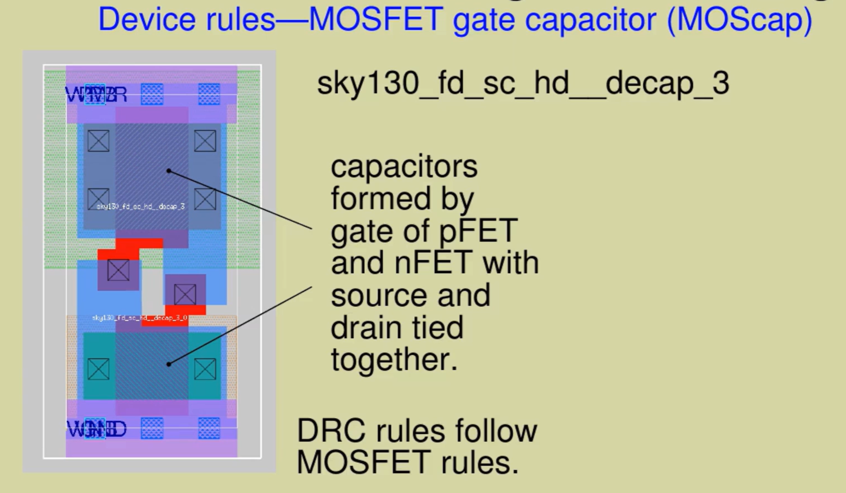
So, in the varactor you have Gate (poly) over NWELL with N+ diffusion, and on the MOSCAP you have a Gate (poly) over PWELL (or PSUB) with N+ diffusion.
And at the end of the day it all translates into a different C-V curve where V is the voltage difference between the 2 terminals. So the varactor is more used for like LC oscillators etc, and the MOSCAP is more for the likes of supply decoupling caps but can be used in many other applications.
It’s a 2 terminal device where the change in capacitance is achieved by just the voltage difference between Gate and Source. Capacitor is formed at the intersection between Gate (poly) and channel (Nwell / N difusion below it). The 2 cap plates are the gate and the source, and the dielectric is the gate oxide.
This is a cross-section of a single-finger NMOS varactor. Note the diffusion is N+ and the well is also NWELL.

Another varactor cross section:

Varactor layers layout view in Magic:

MOSCAPs: It's a transistor with S, D and Bulk connected together.
VPP cap Vertical parallel plate, MOM cap. Notice the inter-digitated structure. Reminds of the crazy TSMC65 “rotating” RT-MOMcap.

Determining the Cap value of a MOM cap by extraction is tricky, and ends up being a poor approximation of the actual value.
THERE IS ALMOST NO REASON TO REASON TO USE MOM CAPS IN A PROCESS THAT HAS MIM CAPS AVAILABLE.
In other processes like 65nm we may not have a MIM cap so we may stick to MOM caps. Let alone 28nm.
MIMcaps MIMcaps can have much more C per unit area, due to the dielectric, they can be much more dense.

Rules around the MiM cap from above:
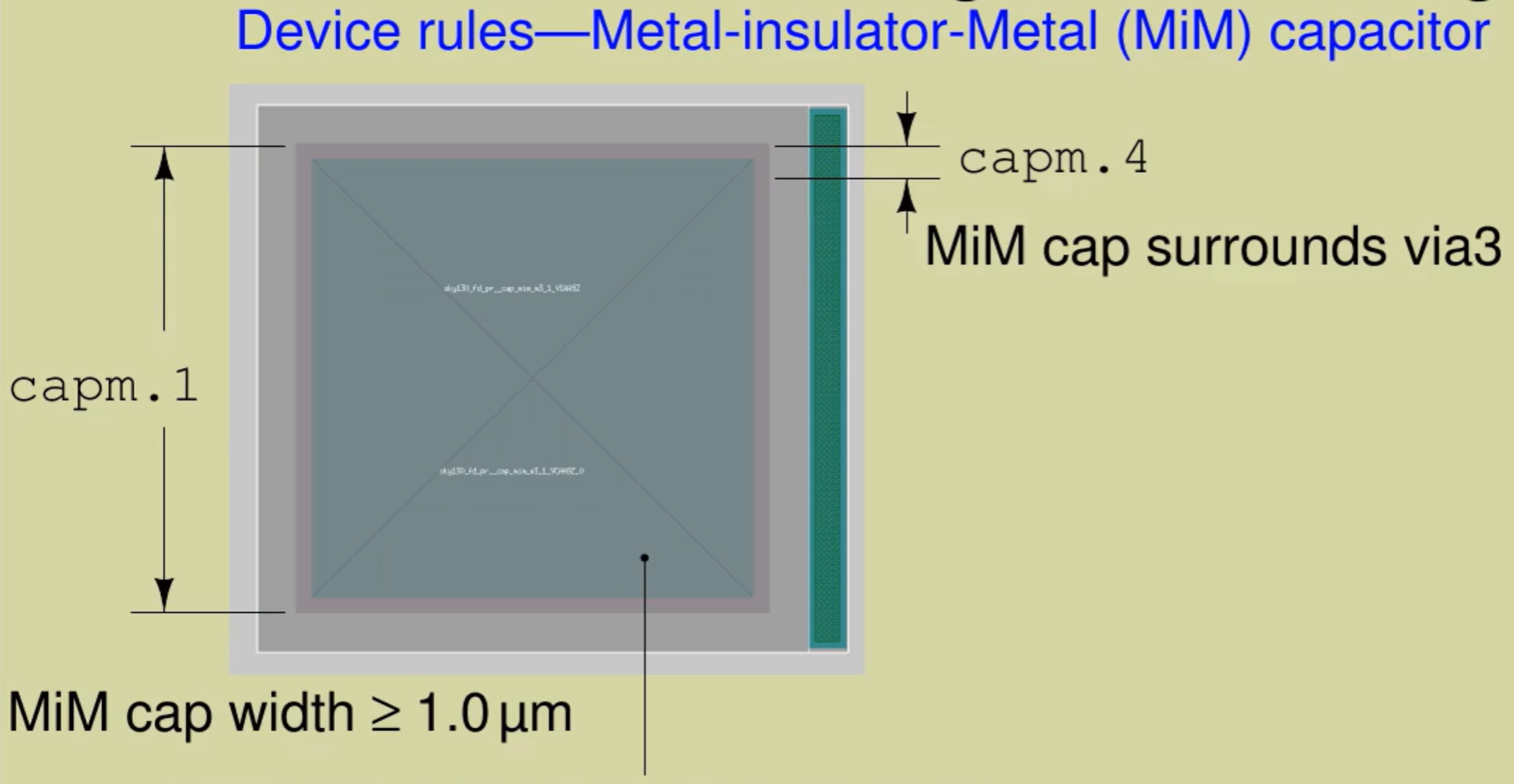
Most MiM cap DRC rules are not so much to avoid breaking it in manufacturing but mostly to ensure the Cap per unit area comes out as the “advertised 1fF per um2”.
You also have “dual layer” MiM caps to be able to stack MiM caps over each other with different metal layers, so you get double capacitance in the same area, although you loose routing capability over it, but if you can route elsewhere then ok.
MiM caps are also subject to antenna rules due to the chunky areas of metal that can accumulate charge during manufacturing.
Diodes:

These are parasitic junction diodes, they are usually unwanted, but in case you actually want a diode by design as a component of your circuit, then you draw it in layout and you put an ID layer over it so that you tell Magic that that is a diode that you have put there on purpose, you want that to be a diode, otherwise Magic may flag it as an unwanted parasitic diode that is not supposed to be in the circuit.
Other than that, you can put down pcell type diodes that come pre-made or parameterized with the PDK, and those are used for like antenna rules etc.
Bipolars: These are fixed layout devices given by the PDK.
Like this PNP bipolar. They are guaranteed to be DRC clean out of the box. Just need to not violate spacing rules around them.

Some layers in Skywater 130 are only ever used in devices that have a fixed layout and the user can never draw anything custom with those layers.
For Skywater 130 that includes layers like the UHV (Ultra High Voltage layer, for those 20V devices), high voltage Extended Drain devices, bipolars, special RF transistors, photodiodes, SRAM core cells, NVRAM cells and other special devices.
These devices are in the skywater130_fd_pr library and have their fixed layouts as GDS. As a designer you just instantiate them with their pre-made fixed layouts and don’t worry about DRC rules for them.
Miscellaneous DRCs: All data must be on 0.005um grid.

Angle limitations: just 90 or 45 degrees.

Seal ring: Seal ring is treated as a fixed layout device, even though the outer seal ring size grows or shrinks depending on die size. But essentially it’s a bunch of fixed layout that are tiled and stretched to form the outer seal ring.

Latch up rules: Avoid PN and PNP junctions to be forward biased.

To avoid this, there are tap to diff distance rules.

Antenna rules: These are to avoid charge accumulation in long metal tracks during manufacturing that would break transistor gates.


To fix antenna violations, you can place diodes which are called “antenna diodes” but which can be really just a simple parasitic junction diode attached to the wire on one end and grounded on the other.

Ideally you could have diodes built into cells. In fact sometimes antenna diodes are put at gates of differential pairs etc.

Another way to avoid antenna violations is to break the metal routing.

Stress avoidance and Slotting rules:

Corners are subject to stress. But essentially these corners of the chip are fixed layout areas, because in the chip corner we usually have fixed layout cells like pad cells which are fixed layout cells and hence are DRC clean by design and the designer doesn’t need to worry about them.

Density rules: Some of these are to ensure the required flatness of the internal chip surfaces.

To meet these rules, we do fill insertion. This is done automatically via fill insertion scripts. After running one of these scripts, you are pretty much guaranteed to have all your density rules correctly covered.

However these inserted fill patterns can add extra capacitance and coupling down to analog circuits underneath and can therefore degrade their performance or even break their functionality.
To avoid this, it is possible to insert blocking layers (“fill block”) in the layout which tell the fill generator script not to put any fill patterns over specific sensitive areas. An example of this is large spiral inductors, or parasitic sensitive VCOs, etc. When you add “fill block” areas, if these areas are large, you could then break the minimum density rule, and then you have to work around that or see if it can be waived or not, etc.

Sometimes you may get a situation in layout where some areas are such that even the fill insertion script can’t insert fill patterns well enough to cover the density rule. Then you may have to tweak the layout in that area.

Also you may break the density rule by having areas with too much metal, scripts can only add fill shapes but not substract, so in this situation you may have to tweak the design manually.

Recommended rules (RR): These are recommendations for improving yield, important for going to production with the chip, not so much for test chips or shuttle runs, but try to cover as many of them as possible.

Your chip won’t be rejected for production due to violating these rules, nor will you be required a waiver for them.
Manufacturing rules vs Test rules: Manufacturing rules are more stringent than test rules.

Rule waivers: You acknowledge the risk of producing your chip with certain rules violated.

ERC (Electrical rule checks): Your design may be DRC clean from the point of view of manufacturability but you still need to check you don’t have ERC problems like electromigration, overvoltage conditions, etc.
Excercise 1: Here we practiced fixing DRC violations related to width, spacing, wide spacing and notches in metals and other layers.

Excercise 2: We practiced fixing rules around Via Size, Multiple Vias, Via Overlap and Autogenerated Vias created by Magic when routing from one metal layer to the metal above or below.
We also learned to use cif see MCON to see the generated contacts that Magic generates in the via areas.

Excercise 3: We practiced fixing DRC violations around minimum area and minimum hole size. Minimum area violations come out in standard cells because their terminals, like gates, are supposed to be connected with metal at the next level above, where they are instantiated.

Excercise 4: We practiced fixing DRCs around wells, NWELLs, well taps and Deep NWELLs. We also learned about the automatic generation of a Deep Nwell area with guardring around it in Magic.

Excercise 5:
We learned how Magic automatically generates layers when it detects overlaps between drawn layers like diffusion and poly to create transistors and other devices. These are called generated layers. These are layers like NSDM, PSDM, etc. which we can see with cif see NSDM, cif see PSDM, cif see LVTN, cif see HVI, etc. If we want to create Low VT devices we need to put down the corresponding LVT layer on the transistor channel so Magic knows we want an LVT device. Same goes for high voltage devices.

Excercise 6: When we instantiate parameterized devices, these may not be DRC clean by themselves, even though they are library cells. This is because they are expected to be made DRC clean at the level above by connecting their ports through metal tracks to other parts of the hierarchy. This is normal and these DRCs go away as soon as we add metal on top of these ports.

Excercise 7: There may be DRCs related to angle errors if angles are not exactly 45 or 90 degrees. Sometimes an angle may look like 45 degrees but in reality it’s not, we can debug this by looking at box dimensions by querying a selected box size.
There may be DRCs also if overlapping via or contact arrays (which are autogenerated by Magic) are coming from different cells in the hierarchy. In such cases we may have to do careful alignment of the vias.

Excercise 8: The seal ring is a fixed layout with some special characteristics and layer usage. In case Magic can’t read a specific cell, because it can’t find it in the filesystem, it may be because the filepath that it is pointing to is different than what we have in our system so Magic can’t find it.
A useful command in Magic is to be able to change the filepath from which Magic tries to find a cell. After selecting the cell in Magic:
select cell: seal_ring_corner_abstract_0
We read the current filepath where Magic is trying to find the cell:
cellname filepath seal_ring_corner_abstract /usr/share/pdk/sky130A/libs.tech/magic/seal_ring_generator
Then we give it a new filepath, the correct one in this case:
cellname filepath seal_ring_corner_abstract /usr/local/share/pdk/sky130A/libs.tech/magic/seal_ring_generator

The seal ring is generated procedurally via a script and then read into Magic. It makes a very non-standard use of the layers. So, what we visualize in Magic is an abstract view of the seal ring that is DRC clean but that does not really look like the real-life seal ring at all, it’s more like a cell with various blockage layers that prevent the user from putting diffusions over it, etc.
We run the seal ring generator script:
usr/local/share/pdk/sky130A/libs.tech/magic/seal_ring_generator/sky130_gen_sealring.py 2000 2000 seal_test
where 2000 x 2000 is the outer chip dimensions and seal_test is the target directory.

The seal ring is generated:


Now we can open this seal ring in Magic. We need to add the path to the seal_test directory so Magic can see it and load it, addpath seal_test and then load advSeal_6um_gen.

To be able to actually see the seal ring layers, we need to launch Magic with a new techfile configuration which is set up to display the process layers from a GDS much more realistically but without DRC information, so then Magic becomes more like a GDS viewer like Klayout.
This is done with the “gds_magic” launch script which is just launching Magic with a different tech file, as seen below:

Then we read the seal ring GDS with gds read seal_test/advSeal_6um_gen
Now we can see the seal ring.

Exercise 9: Importance of tap cells. We expand cells and query them to see the violations report:

These violations are because these are standard cells, are supposed to be handled by place and route tools and tap cells are supposed to be abutted around them.
As soon as we add the appropriate tap cell, with getcell sky130_fd_sc_hd__tapvpwrvgnd_1, the DRCs go away.

Now, regarding the antenna rules.
Since this is an electrical rule check, it requires an extraction first, to gain knowledge of the circuit.
extract do local
extract all
Then:
antennacheck
But that doesn’t give many details, so we run:
antennacheck debug
antennacheck
Now we get details, in particular about the ratio of tracks that caused the violation.

To fix the antenna violation, we can tie down the route to a diffusion through a diode. By doing this and running the antenna check again, we see the antenna violation is fixed.

With see no via2,m3 we can hide layers to see where the problematic antenna tracks are.
Excercise 11:
With cif cover MET1 (or MET2, MET3…) we get the percentage coverage of that metal over the whole layout.

The density checking script looks at a GDS. In Magic we generate a GDS:
gds write excercise_11
Then in a terminal we run the script:
/usr/local/share/pdk/sky130A/libs.tech/magic/check_density.py ./excercise_11.gds
That runs the density checking script:

We now run the “generate_fill.py” script to generate the fill that will fix the density errors.
/usr/local/share/pdk/sky130A/libs.tech/magic/generate_fill.py ./excercise_11.mag

We open the filled GDS in Magic:
gds read exercise_11_fill_pattern.gds.

To see the fill patterns we hide all layers with see no * and then show the metal 2 fill with see m2fill.

Then we load the fill onto the original layout:
box values 0 0 0 0 (this is important, it’s to put the cursor box exactly at the origin)
getcell excercise_11_fill_pattern child 0 0 (this is also important, to ensure the origin of the imported fill pattern aligns with the origin of the original layout)

The OpenLane Flow. OpenLane is an automated RTL to GDSII flow based on several components including OpenROAD, Yosys, Magic, Netgen, Fault and custom methodology scripts for design exploration and optimization. The flow performs full ASIC implementation steps from RTL all the way down to GDSII.
OpenLane Design Flow Stages:
- Synthesis: RTL is converted to Gate level netlist and STA is done.
- RTL synthesis is done with Yosis
- Technology mapping is done with ABC
- Static Timing Analysis is done with OpenSTA.
-
Floorplanning: macros are organized in rows as well as routing tracks, then PDN gets generated and well taps and decap cells are inserted.
-
Placement: macros and cells are placed.
-
CTS: Clock Tree Synthesis is done with TritonCTS.
-
Routing: FastRoute does the global routing, then TritonRoute does the detailed routing and SPEF-Extractor does the SPEF extraction.
-
GDSII generation is done with Magic to stream out the final GDS from the routed def, Klayout is also used.
-
Checks like DRC & Antenna Checks are done in Magic, LVS is done with netgen and CVC is used for circuit validity checks.
Interactive Vs Non-Interactive modes for OpenLane The Openlane flow can be run in Interactive or Non-Interactive modes.
The Non interactive method uses scripts which are run in batch from the terminal in sequence to perform all the stages mentioned above. It is more automated but there is less control at each stage.
The Interactive method lets the user intervene at each stage, verifying the output of each stage and allowing to make any changes if required.
LVS is the process of comparing two netlists, one from layout and one from schematic. This is a good summary of LVS extraction options:

Netgen LVS shell command:

Ideally we would like to run a hierarchical LVS where a schematic hierarchy matches exactly the layout hierarchy. But that is not always the case.

In fact, parameterized devices in layout have a wrapper around them so that alone means a difference in hierarchy between schematic and layout.

So, netgen will “flatten” the hierarchy by including the contents of the cell below into the cell above, and then do the comparison, if the comparison matches then the two hierarchies are equivalent.

Example of this:

To deal with this type of scenario (quite common), netgen creates a queue of subcircuits, from bottom most to top most, comparing them in order from the bottom up.
The problem with this is that if there is a mismatch in a low level cell, netgen will flatten it up into the next level, which will again not match, and that will get flatten again up to the next level, which will not match, and so on, so we get a report where nothing matches, from top to bottom, and we don’t know where the specific mismatch is (in this example it’s in the low level cell C, but we don’t know from the report).

To aid in debugging this kind of situation, tt is possible to tell netgen not to flatten certain cells, by telling it -noflatten=cell_c likely at the lower levels of the hierarchy, so that if those lower level cells don’t match, but the cells above do match, then we have isolated that we have a mismatch at the lower level cell, so we know where to look and where the error needs fixed.

This is how netgen gets told that, for a certain device type, parallel devices can be lumped together into a single device, and that some of its terminals are permutable, etc.

Netgen won’t do network simplification so it must not be assumed that netgen will simplify networks from layout and consider them equivalent to the schematic, because it won’t.

However for resistors we do want netgen to combine them in series/parallel. So, we tell netgen which devices can be combined in series/parallel and with which parameters.
In netgen we can also insert 0V voltage sources or 0 Ohm resistors in the schematic and netgen will still work fine (it will ignore them).
Dummy devices: if netgen sees a device in layout that has all its terminals tied together, then it will consider it’s a dummy device and will ignore it, i.e. you don’t need to have it in the schematic to get a LVS match.

But if a dummy device doesn’t have all terminals tied together, like a transistor with S, D and B tied together but not the gate, then that’s acting as a MOSCAP and hence you need to backannotate it into the schematic.

When it comes to analyzing the LVS results, the output format allows a side by side comparison:

Prior to doing any comparison, netgen will dump a list of which cells it flattened because it couldn’t find any circuit in the opposing netlist to match it to (we talked about this before, things like those wrappers around parameterized devices, etc).

Then netgen will do an attempt to do parallel/series combinations of devices, you will see this in the log here:

Then you get the side by side report. Watch for device counts that have been reduced due to parallel/series combining.

At the end you will see a final sanity check of total number of devices and nets of each side. This is a good place to start when debugging LVS errors.
After that summary, netgen gives you the result of pre-match analysis. Remember the pre-match stage is iterative, it will contain a few iterations, each one with its summary of results in the log, so the first iterations may have errors and that is normal, then on next iteration netgen flattens some cells to see if it can get a better pre-match and run the iteration again, and maybe some of the previous errors are gone in the next iteration, so keep this in mind when visually scanning the log. Erros in some of the initial stages of this pre-match iterative process may be just normal and may not be LVS errors at all, just that netgen was trying to find the good amount of flattening the match both netlists as best as possible.

After that, netgen will present the matching results, it will distinguish between “match” and “unique match”, where match means there were symmetries and matched after breaking those symmetries.

If topology matching succeeds, then you get the result of property matching. Again it may try more parallel/series combinations to try to get the property matching (width of parallel devices, etc).

If the topology and property matching checks both succeed, then netgen does the pin matching check. Always in that order.

If topology matching fails, netgen will dump a list of failing partitions, that gives you a hint of where the mismatch comes from.

General debugging rule of thumb: check DEVICE mismatches first, and if all devices are matching ok, then look at NET mismatches, but ONLY look at NET mismatches after you have all DEVICES matching. This is because if there are DEVICE mismatches, that will produce a long list of NET mismatches as a result, which will go away once the DEVICE mismatch is fixed. So go in that order.
Rule of thumb 2 is that LVS debugging is iterative by nature, so fix the easy and obvious errors first, run LVS again, that will remove many other incomprehensible errors, but will still leave some other errors tackling first the ones that are easy to solve, but go in that order until all LVS errors are gone.

Another important LVS debug skill is to understand where to find the info that will guide you to successfully finding the source of your LVS errors to be able to fix them. That means understanding the run-time output from netgen is not the same as the full log output. The run-time output is just a summary, useful for a quick look, but should not be used for debugging. The full log (comp.out) has the key details and is what you need to use for debugging.

Netgen has a GUI for debug, you can get it running netgen with netgen -gui. The GUI is written in python and it takes the netgen output in json format.

The GUI may be handy for debug sometimes, it’s a bit more visual and it doesn’t truncate circuit names (the log output does).
First quick tests with netgen LVS. We have 2 simple netlists, they are initially the same, we run LVS on them and we get a match. We inspect the log and the comp.out.
Here we run netgen lvs with
netgen lvs netA.spice netB.spice

Then we modify one of the netlists to make them mismatch, we run LVS again and we inspect output logs to see how things look like in case of a mismatch like this.

If the two netlists have .subckt definitions inside them but no subcircuit instantiations, netgen lvs will not run, unless we, along with the two netlist names, give it also the name of the subcircuit to be compared.


For this scenario, we run netgen lvs like this, giving it the name of the subcircuit to be compared:
netgen lvs “netA.spice test” “netB.spice test”
Then the lvs runs and we see the match:

We also see the comp.out circuits and pins are the same:

Pins of the test subcircuit are matching.
Now we modify the pins order in the test subcircuit, and we see that it’s still a exact match, because netgen doesn’t care that the pins are ordered differently as long as internal connectivity is the same between netlists.

But if we now change the internal order of the connections, now netgen sees a mismatch and reports that top level pins are mismatching.


Also here we prepare our run_lvs.sh script which looks like this:

This will produce the json output which is used by the “count_lvs.py” python script and it will append the output of that script to the log, an lvs count summary that looks like this:

Now we deal with empty subcircuit definitions which can be treated as black boxes by netgen.

Initially all cells have matching pins.

But if we change on cell1 the order of pins from A B C to C B A Now we get a mismatch.

Here we see it has treated pin names as meaningful:

Now if we change pin names on cell1 to be A B D instead of A B C, then it finds that D is missing on cell1 in netlistB and C is missing on cell1 in netlistA.

Now, if we change the cell name from cell1 to cell4 in netlistA (leaving pins as A B C), both in the definition and in the instantiation, now we get a unique match again. This is because the cell name is cell4 in netlistA and cell1 in netlisB, but other than that the connectivity is exactly the same in both netlists, so netgen understands that cell4 on netlistA is equivalent to cell1 in netlistB.

In fact, we see it achieves this because first it notices that there is not cell4 in netlisB so it goes ahead and flattens cell4, and then both netlists are equivalent.

If we run lvs with the -blackbox option, it forces netgen to treat cell1 to cell4 as blackboxes, and therefore cell4 is one particular blackbox and cell1 is a different blackbox, so then the lvs shows a mismatch, as now cell4 cannot be flattened or considered equivalent to cell1.

Now we have a netlist with SPICE components (R, C, Diode…) as opposed to just subcircuits (which start by X).

In cell1, we swap out the pins from A B C to C B A. Inside cell1 we only have 2 resistors attached to A B and B C respectively, and resistor terminals are swappable, but netgen still sees a mismatch due to the swapped pins A and C.
That’s because we have not told netgen that for cell1 pins A and C are permutable. We need to tell it so in the setup.tcl file, as follows: At the bottom of the setup.tcl file:

Inside the .sh run script, use the new .tcl:

Now we get a match.

That’s because in cell1 there are resistors which are swappable, but in cell3 we have diodes which aren’t swappable, so if we swap pin names on cell3 (while at the same time swapping internal net connections to keep overall connectivity in cell3) and run that past lvs, it passes lvs this time.
Then we move to an example POR circuit from Caravel analog project.

If we netlist directly from xschem by pressing Netlist buttom directly, we get a netlist but it’s not proper for lvs, since it has a top level subcircuit definition commented out at the top.

So in xschem we need to enable Simulation → “LVS netlist: Top level is a .subckt”, then we can Netlist.

Now the top level .subckt is not commented out:

In this netlist, transistors and also resistors are not simple SPICE primitives but subcircuits, this is standard practice in PDKs.
In order to tell netgen to treat these particular subcircuits as if they were low level primitives, we need to tell it to do so, and we do that in the setup.tcl file that netgen uses.
For example, that file contains some Tcl loops to inform netgen that it is fine to do some pin permutations, parallel/series combinations, etc, for certain subcircuits that we want netgen to treat as a low level primitives.

Now we open the circuit layout and we extract the netlist from the layout, for LVS.
extract do local
extract all
ext2spice lvs
ext2spice

We then run netgen LVS with the provided run_lvs_wrapper.sh:

We get some mismatches.

Inside the comp.out we see the cause of the LVS mismatch is due to the standard cells:

Standard cells are not included in the schematic netlist, and without a proper subcircuit definition netgen just names the standard cell pins as 1, 2, 3, … 6, whereas in the layout standard cells appear as proper subcircuits with their pins named with sensible names, and netgen considers they are not necessarily the same thing on both sides, so it propagates the pin name mismatch to the top level and thus the LVS ends up not being clean.
So we need to provide a proper subcircuit definition for the standard cells.
We will get that from the corresponding testbench that is supposed to test this schematic.

From that TB we see it has a block of code with includes for the standard cell libraries. We netlist this TB (no need to enable the Simulation LVS blabla option this time) and therefore we get those standard cell include lines printed into the netlist.

We will LVS the layout agains this netlist now.

Now we get the LVS match, except for some unmatched pins.

Now we run the netgen LVS with a run script that tells netgen to compare the LVS not of the top level but of the “example_por” cell that is instantiated in the schematic.

And we see the “example_por” cells are LVS clean.

These are the pin mismatches in the wrapper:


Important shortcut key in Magic, s s s to select a whole net, important for tracing through the layout along various layers.
We find that io_analog[4] is tied to io_clamp_high[0], not an error but two pins on same metal track, so let’s split them by a metal 3 resistor shortcircuit (paint rmetal3).


The same resistor must be added to the schematic in xschem:

Then we can netlist again and run LVS again. Still there are 9 pins mismatching due to being shorted to vssa1 and vssd1 in the layout, and therefore need resistors added to separate the two nets as well. Again, we need to add equivalent resistors in xschem, then run netgen lvs again will get it LVS clean.
Another important command in Magic is goto {io_oeb[11]} (name of the desired pin between brackets) and that will let us zoom into the right pin. Once that is selected, we can type getnode and that will tell us what net that pin is connected to, and se can see the shorts to vssd1.
Excercise 6: We are going to LVS a layout against a verilog netlist, in this case a digital PLL. First we extract the layout netlist and we run LVS agains the verilog netlist “digital_pll.v” which is a verilog netlist (i.e. not behavioural verilog but a netlist). LVS fails and upon looking at the log we see missing fill cells and tap cells in the layout:

We see that the fill cells in the verilog netlist are called FILLER_0_11, we search for any of those in the extracted layout netlist to see if they are there or not, but it’s not there.
We go back to Magic to see if that FILLER_0_11 is there or not, we search for it with (important Magic command):
select FILLER_0_11
And indeed it’s there.

If we push (descend) into the cell with > key, we see it’s a quite simple thing so what happens is that the extractor has optimized it out because it doesn’t have any active device or anything “circuit-like”.
To fix this, we edit the netgen setup.tcl file. We find the section where it talks about fill.

We are going to assume that this layout (for digital_pll.v or similar placed-and-routed layout) comes from a PNR tool, rather than from a human. Hence we are going to assume the PNR tool is fine enough that we can trust it will never put fill and tap cells in any wrong place, or upside down, or overlapping something else causing a short, or an open, etc… So we are going to make it so that netgen completely ignores these fill cells. For that, we set this environment variable MAGIC_EXT_USE_GDS. We put it inside netgen’s setup.tcl file.

And that way we get a match!

Excercise 9: LVS with property errors. After extracting the layout and netlisting the schematic, we run LVS and see property errors in some devices.

We use this information to see exactly what caps, resistors and transistors we need to edit, in this case in the schematic, to get the LVS match again.
For the resistors and caps, we change their properties in the schematic.

For the transistor, we change it in the layout from 2 fingers to 1 finger. For this, we first locate the specific transistor which is sky130_fd_pr__nfet_g5v0d10v5_8KW54N_0.

And we get an LVS match.

Skywater 130 PDK: https://github.com/google/skywater-pdk
Open_PDKS: http://www.opencircuitdesign.com/open_pdks/
VSD Physical Verification using SKY130: https://www.vlsisystemdesign.com/physical-verification-using-sky130/