Processing in memory (PIM) aims at improving computational speed by bringing the computational engine to memory and avoid the energy consumption associated with existing von Neumann style of computing. Improve in compute ability by reduction in transistor size is approaching its limit, and with increase in compute intensive tasks involved with edge computing, IoT applications etc. we need to look for alternative techniques like – In/near memory computing. In this paper we will perform logical operations using 8TSRAM cells to overcome the von Neumann bottleneck.
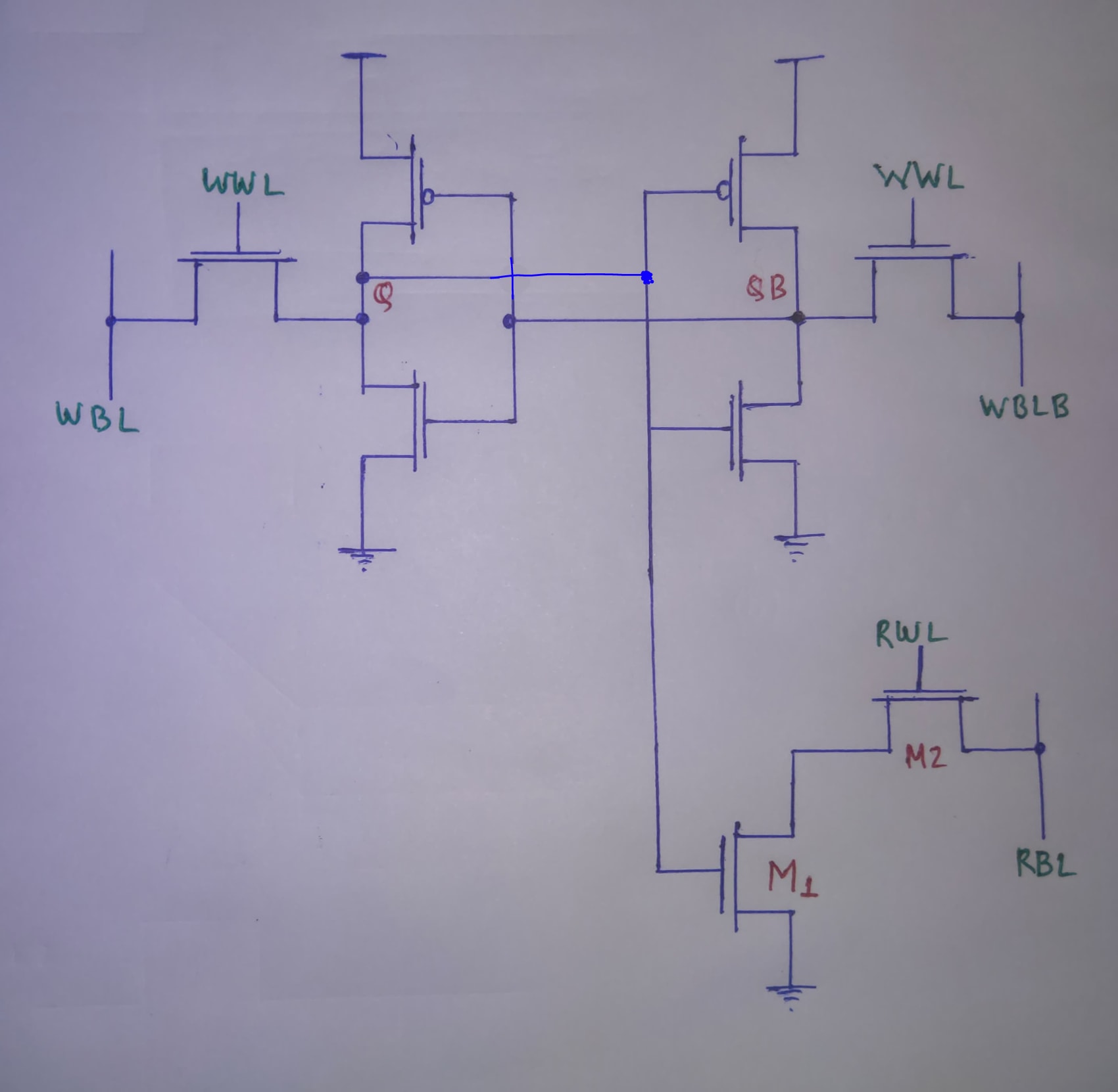 Fig1. 8TSRAM cell
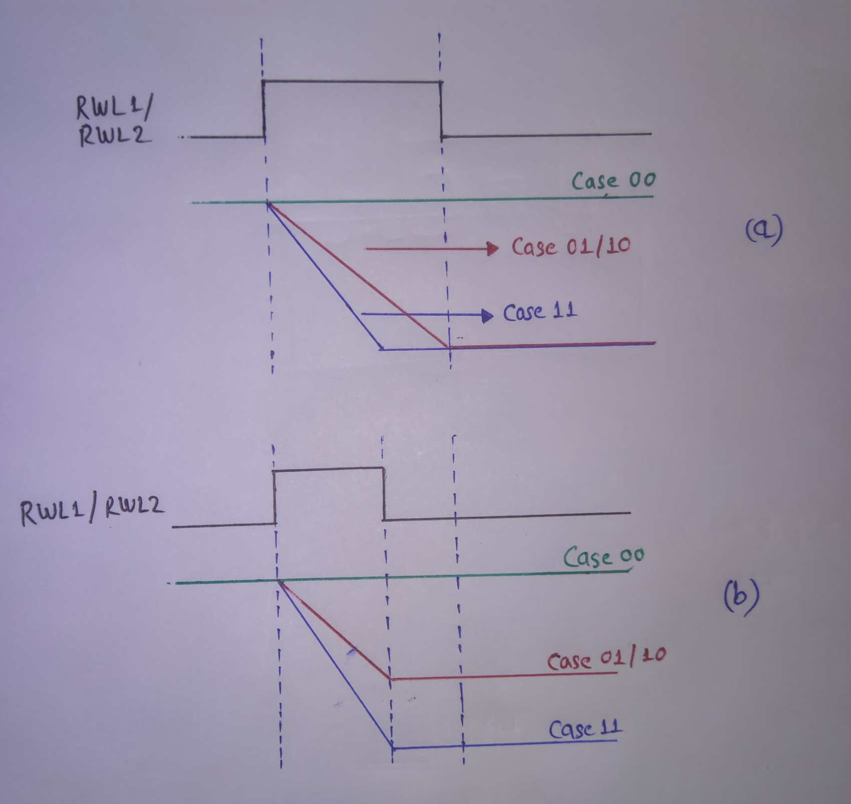 Fig 2. Timing analysis
 Fig 3. Overall design

8TSRAM cells are written with values either 0 or 1. The value stored is then fed to the read circuitry of 8TSRAM cells(Gate of the nfets) The RBL(Read Bit line) capacitor is precharged. Both 8TSRAM cells are written with 0 or 1, which is equivalent to providing input to a logic GATE. After the values are written, a read bit line enable mosfet switches on. This happens together with a read word line being enabled. This allows the precharged capacitor to discharge via any of the two nfets if their gate potential is high( gate potential high means that 8TSRAM cell has logic 1 written to it). This makes the precahrged capacitor potential mimic a logic value corresponding to a NOR operation. This NOR output from capacitor is input to a CMOS inverter to generate an OR operation. The verilog code of MUX gets input Data[1:0]. When Sel(select line) is 1 the output from the analog port generating logic operation OR is chosen. When Sel is 0 the output from the analog port generating NOR is chosen.
module rahul_mux(data, sel, out);
input [1:0] data; input sel; output out;
assign out = sel?data[1]:data[0];
endmodule
\TLV_version 1d: tl-x.org
\SV
/* verilator lint_off UNUSED*/ /* verilator lint_off DECLFILENAME*/ /* verilator lint_off BLKSEQ*/ /* verilator lint_off WIDTH*/ /* verilator lint_off SELRANGE*/ /* verilator lint_off PINCONNECTEMPTY*/ /* verilator lint_off DEFPARAM*/ /* verilator lint_off IMPLICIT*/ /* verilator lint_off COMBDLY*/ /* verilator lint_off SYNCASYNCNET*/ /* verilator lint_off UNOPTFLAT / / verilator lint_off UNSIGNED*/ /* verilator lint_off CASEINCOMPLETE*/ /* verilator lint_off UNDRIVEN*/ /* verilator lint_off VARHIDDEN*/ /* verilator lint_off CASEX*/ /* verilator lint_off CASEOVERLAP*/ /* verilator lint_off PINMISSING*/ /* verilator lint_off BLKANDNBLK*/ /* verilator lint_off MULTIDRIVEN*/ /* verilator lint_off WIDTHCONCAT*/ /* verilator lint_off ASSIGNDLY*/ /* verilator lint_off MODDUP*/ /* verilator lint_off STMTDLY*/ /* verilator lint_off LITENDIAN*/ /* verilator lint_off INITIALDLY*/
//Your Verilog/System Verilog Code Starts Here:
module rahul_mux(data, sel, out);
input [1:0] data; input sel; output out;
assign out = sel?data[1]:data[0];
endmodule
//Top Module Code Starts here: module top(input logic clk, input logic reset, input logic [31:0] cyc_cnt, output logic passed, output logic failed); logic [1:0] data;//input logic sel;//input logic out;//output //The $random() can be replaced if user wants to assign values assign data = $random(); assign sel = $random(); rahul_mux rahul_mux(.data(data), .sel(sel), .out(out));
\TLV
//Add \TLV here if desired
\SV
endmodule
-
/home/tiw.rahul45/eSim-Workspace/LOGICwithSRAM/LOGICwithSRAM.cir
-
EESchema Netlist Version 1.1 (Spice format) creation date: Sat 08 Oct 2022 09:16:51 PM IST
-
To exclude a component from the Spice Netlist add [Spice_Netlist_Enabled] user FIELD set to: N
-
To reorder the component spice node sequence add [Spice_Node_Sequence] user FIELD and define sequence: 2,1,0
-
Sheet Name: / SC7 Net-SC4-Pad2 Q1 Net-SC4-Pad3 Net-SC4-Pad3 sky130_fd_pr__pfet_01v8 SC4 Q1 Net-SC4-Pad2 Net-SC4-Pad3 Net-SC4-Pad3 sky130_fd_pr__pfet_01v8 SC8 Net-SC4-Pad2 Q1 GND GND sky130_fd_pr__nfet_01v8 SC5 Q1 Net-SC4-Pad2 GND GND sky130_fd_pr__nfet_01v8 SC9 WBLB1 WWL Net-SC4-Pad2 GND sky130_fd_pr__nfet_01v8 SC2 Q1 WWL WBL1 GND sky130_fd_pr__nfet_01v8 v3 Net-SC4-Pad3 GND DC v6 WBLB1 GND pulse v1 WBL1 GND pulse SC13 Q2 Net-SC13-Pad2 Net-SC13-Pad3 Net-SC13-Pad3 sky130_fd_pr__pfet_01v8 SC15 Net-SC13-Pad2 Q2 Net-SC13-Pad3 Net-SC13-Pad3 sky130_fd_pr__pfet_01v8 SC16 Net-SC13-Pad2 Q2 GND GND sky130_fd_pr__nfet_01v8 SC14 Q2 Net-SC13-Pad2 GND GND sky130_fd_pr__nfet_01v8 SC12 Q2 WWL WBL2 GND sky130_fd_pr__nfet_01v8 SC17 WBLB2 WWL Net-SC13-Pad2 GND sky130_fd_pr__nfet_01v8 v8 Net-SC13-Pad3 GND DC v9 WBLB2 GND pulse v7 WBL2 GND pulse SC23 GND Q2 Net-SC22-Pad1 GND sky130_fd_pr__nfet_01v8 SC22 Net-SC22-Pad1 RWL NOR GND sky130_fd_pr__nfet_01v8 SC20 GND Q1 Net-SC19-Pad1 GND sky130_fd_pr__nfet_01v8 SC19 Net-SC19-Pad1 RWL NOR GND sky130_fd_pr__nfet_01v8 v10 RWL GND pulse SC21 NOR GND sky130_fd_pr__cap_mim_m3_1 U2 Q1 plot_v1 U7 Q2 plot_v1 U4 NOR plot_v1 U1 WBL1 plot_v1 U6 WBL2 plot_v1 U8 WBLB2 plot_v1 U9 RWL plot_v1 scmode1 SKY130mode U5 WBLB1 plot_v1 v12 RBLpre GND pulse v2 WWL GND pulse U3 WWL plot_v1 SC1 RBLpre RBLpreEn NOR Net-SC1-Pad4 sky130_fd_pr__pfet_01v8 v5 Net-SC1-Pad4 GND DC v4 RBLpreEn GND pulse U10 RBLpre plot_v1 U11 RBLpreEn plot_v1 X11 NOR Net-U13-Pad1 rahul_inv X12 Net-U13-Pad1 Net-U15-Pad1 rahul_inv U13 Net-U13-Pad1 Net-U12-Pad1 adc_bridge_1 U15 Net-U15-Pad1 Net-U12-Pad2 adc_bridge_1 U12 Net-U12-Pad1 Net-U12-Pad2 Net-U12-Pad3 Net-U12-Pad4 rahul_mux U14 SEL Net-U12-Pad3 adc_bridge_1 v11 SEL GND pulse U16 Net-U12-Pad4 LOGIC dac_bridge_1 U17 LOGIC plot_v1 U18 SEL plot_v1
.end
-
Both SRAM cells written with 1

-
Both SRAM cells are written with 0

-
When the cells are written with 0 and 1
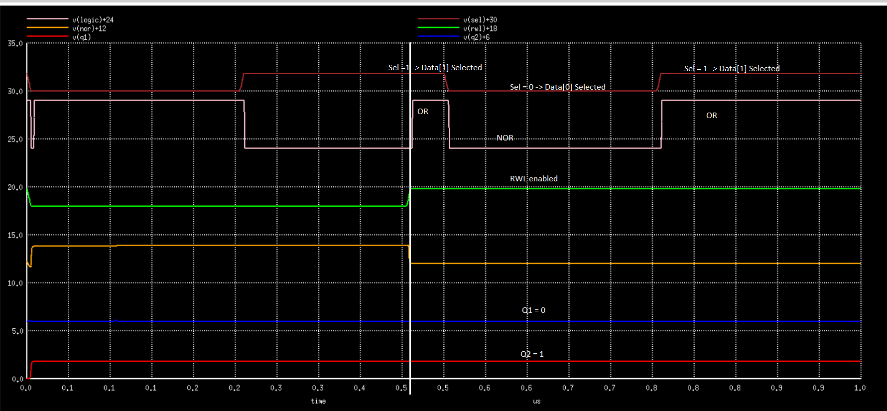
The logic operation starts after the Read word line is enabled. It is shown by the white line that runs vertically throught the plot. SInce input to MUX is both the Logic NOR and Logic OR, variation in select line results in different outputs(logic operations NOR and OR)
The below plots are for the case where bith 8TSRAM cells are written with 1.
 Fig1
Fig1
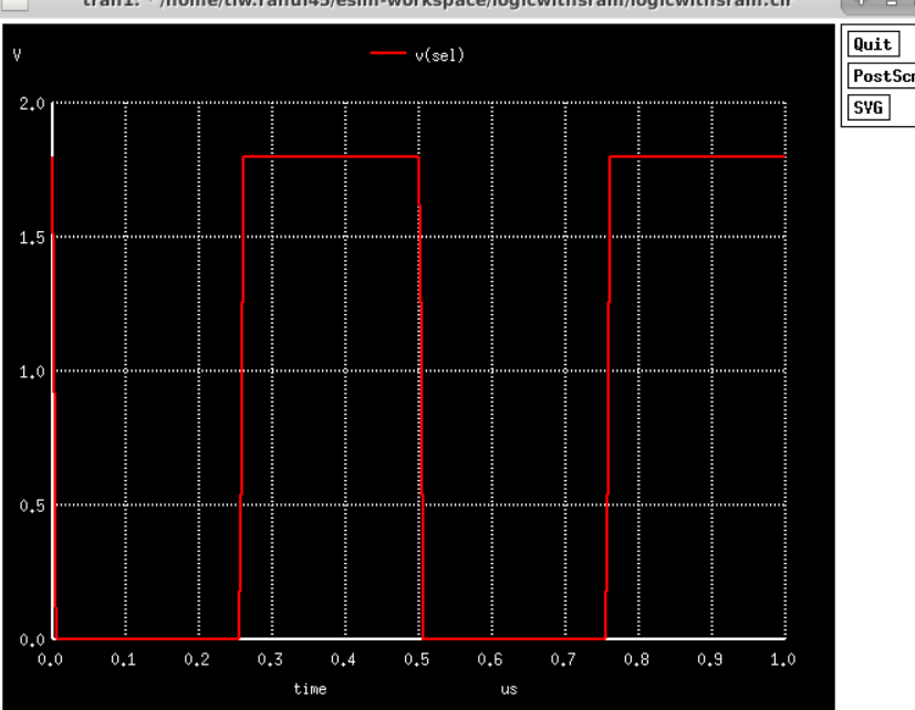 Fig2
Fig2
 Fig3
Fig3
 Fig4
Fig4
 Fig5
Fig5
 Fig6
Fig6
 Fig7
Fig7
 Fig8
Fig8
Fig1. Precharging of read bit line
Fig2. Mux select line variation
Fig3. Output Logic
Fig4. NOR capacitor voltage variation
Fig5. 8TSRAM Cell1 written with 1
Fig6. 8TSRAM Cell2 wrritten with
Fig7. Read Word Line
Fig8. Read Bit Line precharge enable(PMOS switch)
- Open eSim
- Run NgVeri-Makerchip
- Add top level verilog file in Makerchip Tab, and confirm waveform
- Click on NgVeri tab, convert verilog to ngspice, model created successfully
- Make schematic on esim, integrate subcircuit of inverter created seperately. The 8TSRAM cells can also be present int he schematic in subcircuit form.
- Debug for errors, by ERC checks, ignore conflict errors and global label errors, generate netlist, convert kicad to ngspice
- Provide source informations, sky130 component library information, path to any subcircuits used
- Generate simulation
The above project is a demosntration of PIM with SRAM cells. Different device research is going on to support PIM like memristors and work on near memory computing is also being done. The project can be scaled to implement algorithms entirely using SRAM cells. NAND and AND operations have been skipped as it requires further analysis and schematic implemntation. Drawback of PIM using SRAM cells is the large area the cells take.
- FOSSEE, IIT Bombay
- Steve Hoover, Founder, Redwood EDA
- Kunal Ghosh, Co-founder, VSD Corp. Pvt. Ltd. - kunalpghosh@gmail.com
- Sumanto Kar, eSim Team, FOSSEE
[1] Amogh Agrawal, Akhilesh Jaisawal, Chankyu Lee and Kaushik Roy, “X-SRAM: Enabling In-memory Boolean Computations in CMOS Static Random Access Memories”. Circuits and Systems I: Regular Papers, IEEE Transactions on PP(99), December 2017 [2] Sparsh Mittal, Gaurav Verma, Brajesh Kaushik, Farooq A. Khanday, “A Survey of SRAM-based Processing-in-Memory Techniques and Applications”. Journal of Systems Architecture, Volume 119, October 2021, 102276