This work presents a 4-bit ALU with reusable datapaths. It was designed based on 28nm technology node using Synopsys Custom Compiler and simulated using Primewave.
Arithemetic and Logic Unit (ALU) is the heart of a computer which performs all the arithmetics operations such as addition and subtraction and also logical operations such as AND, OR, XOR. The ALU presented here is a fully combinational with reusable datapath, meaning the ciruits can be reused to perform diferent operations.
- Synopsys Custom Compiler: The Synopsys Custom Compiler™ design environment is a modern solution for full-custom analog, custom digital, and mixed-signal IC design. As the heart of the Synopsys Custom Design Platform, Custom Compiler provides design entry, simulation management and analysis, and custom layout editing features. This tool was used to design the circuit on a transistor level.
- Synopsys Primewave: PrimeWave™ Design Environment is a comprehensive and flexible environment for simulation setup and analysis of analog, RF, mixed-signal design, custom-digital and memory designs within the Synopsys Custom Design Platform. This tool helped in various types of simulations of the above designed circuit.
- Synopsys 28nm PDK: The Synopsys 28nm Process Design Kit(PDK) was used in creation and simulation of the above designed circuit.
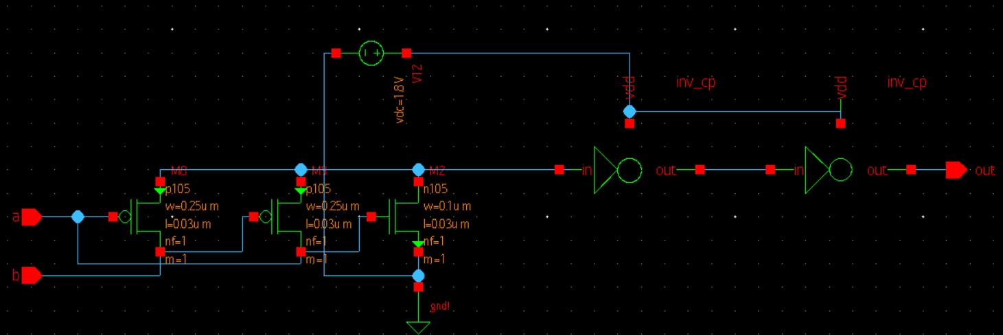
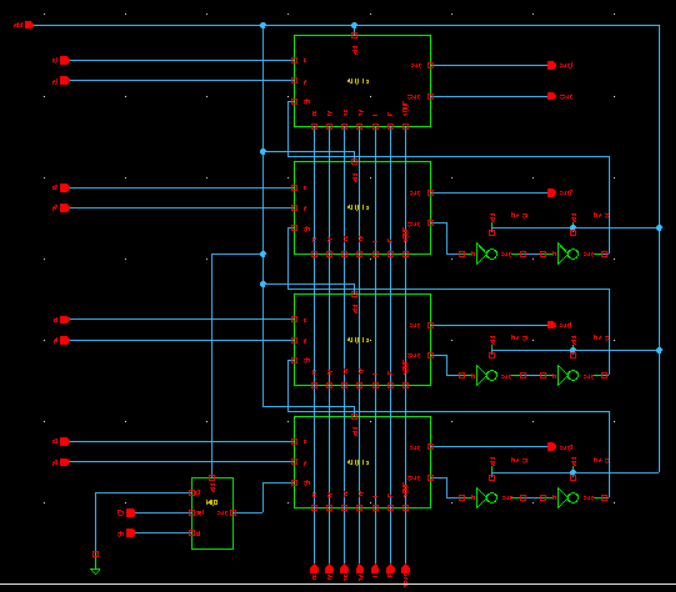
The ALU has 2 4-bit inputs X and Y, one output OUT and 8 control signals zX, zY, nX, nY, L, F, Cs, nOUT. These control signals specify the operation the ALU has to perform. Usually an ALU has N:1 multiplexer which selects the operation based on the select lines. The ALU presented here uses a series of multiplexers to have reusable circuits. The multiplexers are designed using transmission gate to reduce power consumption.

The control signals specify a type of operation:
- zX and zY: If HIGH then it passes 0 to next stage
- nX and nY: If HIGH then it passes inverted input to next stage
- L: Specifies if AND / XOR gate is selected
- F: Specifies if logical operation or adder has to be selected
- Cs: Specifies if carry_in needs to be used or not
- nOUT: If HIGH then it passes inverted input to output
For example, let us take the example of AND operation, this is done by making: zX and zY low (to pass actual inputs), nX and nY low (to not invert them), L and F low (to select AND operation), Cs low (not applicable for current example) and nOUT low (to not invert them).
To do NAND, take the same values of the control signals but make nOUT HIGH to invert the ANDed value.
To do OR operation, we will use De-Morgans Law : ~(~a.~b) = a|b
Hence the control signals will be zX=zY=0, nX=nY=1, L=F=0,Cs=0, nOUT=1.
The below table has a list of common operations and the values of control signals corresponding to it:
| zX | zY | nX | nY | L | F | Cs | nOUT | OPERATION |
|---|---|---|---|---|---|---|---|---|
| 0 | 0 | 0 | 0 | 0 | 0 | 0 | 0 | X&Y |
| 0 | 0 | 0 | 0 | 0 | 0 | 0 | 1 | ~(X&Y) |
| 0 | 0 | 1 | 1 | 0 | 0 | 0 | 1 | X|Y |
| 0 | 0 | 1 | 1 | 0 | 0 | 0 | 0 | ~(X|Y) |
| 0 | 0 | 0 | 0 | 1 | 0 | 0 | 0 | X^Y |
| 0 | 0 | 0 | 0 | 1 | 0 | 0 | 1 | ~(X^Y) |
| 0 | 0 | 0 | 0 | 0 | 1 | 0 | 0 | X+Y |
| 0 | 0 | 0 | 0 | 0 | 1 | 1 | 0 | X+Y+c |
| 0 | 0 | 1 | 0 | 0 | 1 | 0 | 1 | X-Y |
| 0 | 0 | 0 | 1 | 0 | 1 | 0 | 1 | Y-X (borrow) |
| 1 | 0 | 1 | 0 | 0 | 1 | 0 | 1 | -Y |
| 0 | 1 | 1 | 1 | 0 | 1 | 0 | 1 | X+1 |
| 1 | 0 | 1 | 1 | 0 | 1 | 0 | 1 | Y+1 |
| 0 | 1 | 0 | 1 | 0 | 1 | 0 | 0 | X-1 |
| 1 | 0 | 1 | 0 | 0 | 1 | 0 | 0 | Y-1 |


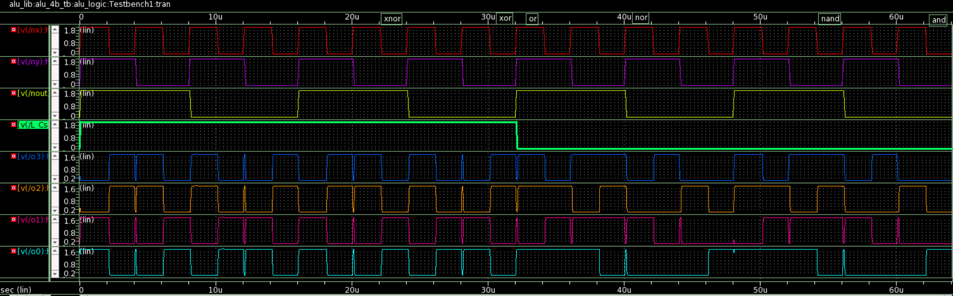
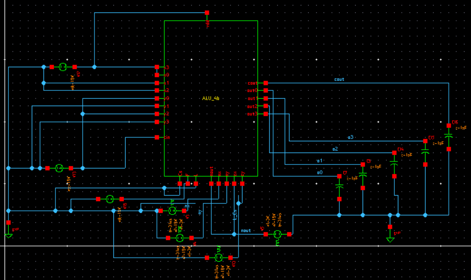
I have made F=1, Cin=1 and L=0. Below are schematic and waveform.


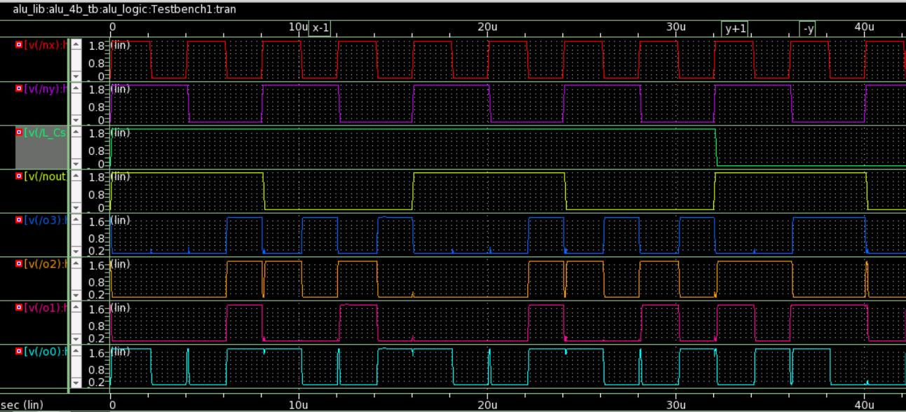
We can ignore the spikes in actual CPU because the data will be held in flipflops and these spikes do not conform to setup and hold times, hence will not cause any issues. Sanchith V M
- Kunal Ghosh, VSD
- Synopsys India
- IIT Hyderabad
- Chinmay Panda, IIT-H
- Sumanto Kar
- Sameer Durgoji, NIT-K
2. Subodh Wairya, Rajendra Kumar Nagaria, Sudarshan Tiwari, "Performance Analysis of High Speed Hybrid CMOS Full Adder Circuits for Low Voltage VLSI Design", VLSI Design, vol. 2012, Article ID 173079, 18 pages, 2012. https://doi.org/10.1155/2012/173079
3. V. Venkata Roa, et al., Design and Simulation of 1-bit Arithmetic Logic Unit using Pass Transistor Logic Families, International Journal of Pure and Applied Mathematics, Volume 120, No. 6 2018