Final Submission of 'google iitb esim mixed signal hackathon'
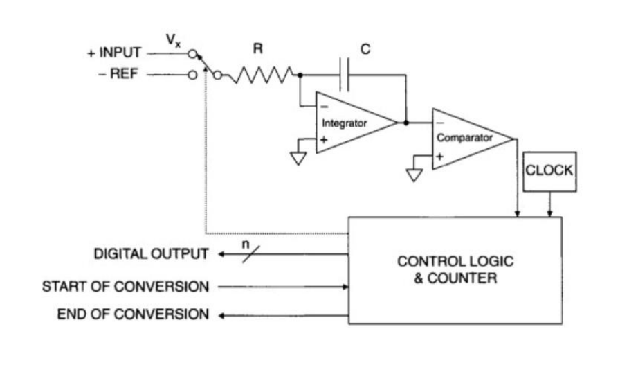
In this paper I have explained an 8-bit dual slope ADC (analog to digital converter) circuit which I have designed. A dual slope ADC produces an equivalent digital output for a corresponding analog input by using two (dual) slope technique. The dual slope ADC mainly consists of 5 blocks: Integrator, Comparator, Clock signal generator, Control logic and Counter
The input signal is applied to an integrator; at the same time a counter is started, counting clock pulses. After a predetermined amount of time (T), a reference voltage having opposite polarity is applied to the integrator. At that instant, the accumulated charge on the integrating capacitor is proportional to the average value of the input over the interval T. The integral of the reference is an opposite-going ramp having a slope of VREF/RC. At the same time, the counter is again counting from zero. When the integrator output reaches zero, the count is stopped, and the analog circuitry is reset. Since the charge gained is proportional to VIN × T, and the equal amount of charge lost is proportional to VREF × tx, then the number of counts relative to the full scale count is proportional to tx/T, or VIN/VREF. If the output of the counter is a binary number, it will therefore be a binary representation of the input voltage. The charge on the capacitor at time t1 is proportional to the average value of Vx times t1. This is equal to the charge lost by the capacitor during time t2 – t1, while being discharged by the reference voltage, proportional to Vr times (t2 – t1). Hence (t2 – t1)/t1 is proportional to Vx/Vr The output binary count for the time interval (t2 – t1) is thus proportional to Vx, the input voltage. With appropriate circuitry, bipolar voltages can also be measured. Dual-slope integration has many advantages. Conversion accuracy is independent of both the capacitance and the clock frequency, because they affect both the up-slope and the down-slope by the same ratio.


As we can see that the final waveform does not match the initial waveform. The circuit which I have designed is not working properly due to the malfunctioning in the integrator block. While trying to debug, i found out that the integrator block was not giving integrating output. That is because of the incorrect W and L values of the respective resistor and capacitor. So, if someone is able to calculate the correct values of W and L,he/she can make the circuit run properly and get the required waveform.
module ritam_control(output reg reset, clk_en,input cin, sw);

initial begin
reset = 0;
clk_en = 1;
end

always @(posedge sw) begin
reset = 1;
end

always @(negedge cin)begin
clk_en = 0;

end

endmodulemodule ritam_counte(output reg [7:0] dout,output reg overflow, input c_en, clk, reset );
initial begin
overflow = 1'b0;
dout = 8'd0;
end
always @(posedge reset)begin
dout = 8'd0;
end
always @(posedge clk)begin
if(c_en) begin
{ overflow, dout} = dout + 8'd1;
end
end
endmodulemodule ritam_start(output sw, input [7:0] a);
assign sw = (!a[7]) & (!a[6]) & (!a[5]) & (!a[4]) & (a[3]) & (!a[2]) & (a[1]) & (!a[0]);
endmodule* c:\users\ritam\esim-workspace\adc\adc.cir
.include avsd_opamp.sub
.include "C:\FOSSEE\eSim\library\sky130_fd_pr\models\sky130_fd_pr__model__pnp.model.spice"
.include "C:\FOSSEE\eSim\library\sky130_fd_pr\models\sky130_fd_pr__model__diode_pd2nw_11v0.model.spice"
.include "C:\FOSSEE\eSim\library\sky130_fd_pr\models\sky130_fd_pr__model__linear.model.spice"
.include "C:\FOSSEE\eSim\library\sky130_fd_pr\models\sky130_fd_pr__model__r+c.model.spice"
.include "C:\FOSSEE\eSim\library\sky130_fd_pr\models\sky130_fd_pr__model__inductors.model.spice"
.lib "C:\FOSSEE\eSim\library\sky130_fd_pr\models\sky130.lib.spice" tt
.include "C:\FOSSEE\eSim\library\sky130_fd_pr\models\sky130_fd_pr__model__diode_pw2nd_11v0.model.spice"
v3 net-_x1-pad1_ gnd dc 3.3
xsc4 out net-_sc3-pad2_ sky130_fd_pr__cap_mim_m3_2 W=10L=1
xsc3 net-_sc1-pad1_ net-_sc3-pad2_ gnd sky130_fd_pr__res_generic_nd W=1 L=10
* u4 net-_u4-pad1_ net-_u2-pad1_ net-_u1-pad3_ net-_u1-pad1_ ritam_control
* u1 net-_u1-pad1_ net-_u1-pad2_ net-_u1-pad3_ net-_u1-pad4_ net-_u1-pad5_ net-_u1-pad6_ net-_u1-pad7_ net-_u1-pad8_ net-_u1-pad9_ net-_u1-pad10_ net-_u1-pad11_ ? ritam_counte
* u5 net-_u1-pad4_ net-_u1-pad5_ net-_u1-pad6_ net-_u1-pad7_ net-_u1-pad8_ net-_u1-pad9_ net-_u1-pad10_ net-_u1-pad11_ net-_u2-pad1_ ritam_start
xsc1 net-_sc1-pad1_ net-_sc1-pad2_ vref vref sky130_fd_pr__nfet_01v8 W=1 L=1
xsc2 net-_sc1-pad1_ net-_sc1-pad2_ vin vin sky130_fd_pr__pfet_01v8 W=1 L=1
v2 vin gnd dc 4
v1 gnd vref dc 5
v4 net-_u7-pad1_ gnd pulse(0 1.8 0 0 0 1u 2u)
* u6 net-_u6-pad1_ net-_u4-pad1_ adc_bridge_1
* u2 net-_u2-pad1_ net-_sc1-pad2_ dac_bridge_1
* u3 out plot_v1
* u7 net-_u7-pad1_ net-_u1-pad2_ adc_bridge_1
* s c m o d e
x1 net-_x1-pad1_ net-_x1-pad2_ net-_sc3-pad2_ gnd out gnd avsd_opamp
v5 gnd net-_x1-pad2_ dc 3.3
x2 net-_x1-pad1_ gnd out gnd net-_u6-pad1_ gnd avsd_opamp
a1 [net-_u4-pad1_ ] [net-_u2-pad1_ ] [net-_u1-pad3_ ] [net-_u1-pad1_ ] u4
a2 [net-_u1-pad1_ ] [net-_u1-pad2_ ] [net-_u1-pad3_ ] [net-_u1-pad4_ net-_u1-pad5_ net-_u1-pad6_ net-_u1-pad7_ net-_u1-pad8_ net-_u1-pad9_ net-_u1-pad10_ net-_u1-pad11_ ] [? ] u1
a3 [net-_u1-pad4_ net-_u1-pad5_ net-_u1-pad6_ net-_u1-pad7_ net-_u1-pad8_ net-_u1-pad9_ net-_u1-pad10_ net-_u1-pad11_ ] [net-_u2-pad1_ ] u5
a4 [net-_u6-pad1_ ] [net-_u4-pad1_ ] u6
a5 [net-_u2-pad1_ ] [net-_sc1-pad2_ ] u2
a6 [net-_u7-pad1_ ] [net-_u1-pad2_ ] u7
* Schematic Name: ritam_control, NgSpice Name: ritam_control
.model u4 ritam_control(rise_delay=1.0e-9 fall_delay=1.0e-9 input_load=1.0e-12 instance_id=1 )
* Schematic Name: ritam_counte, NgSpice Name: ritam_counte
.model u1 ritam_counte(rise_delay=1.0e-9 fall_delay=1.0e-9 input_load=1.0e-12 instance_id=1 )
* Schematic Name: ritam_start, NgSpice Name: ritam_start
.model u5 ritam_start(rise_delay=1.0e-9 fall_delay=1.0e-9 input_load=1.0e-12 instance_id=1 )
* Schematic Name: adc_bridge_1, NgSpice Name: adc_bridge
.model u6 adc_bridge(in_low=1.0 in_high=1.5 rise_delay=1.0e-9 fall_delay=1.0e-9 )
* Schematic Name: dac_bridge_1, NgSpice Name: dac_bridge
.model u2 dac_bridge(out_low=0 out_high=3.3 out_undef=0.5 input_load=1.0e-12 t_rise=1.0e-9 t_fall=1.0e-9 )
* Schematic Name: adc_bridge_1, NgSpice Name: adc_bridge
.model u7 adc_bridge(in_low=1.0 in_high=1.5 rise_delay=1.0e-9 fall_delay=1.0e-9 )
.tran 0.1e-06 10e-06 0e-00
* Control Statements
.control
run
print allv > plot_data_v.txt
print alli > plot_data_i.txt
plot v(out)
.endc
.end(1) Dual Slope Converters, Hank Zumbahlen, with the engineering staff of Analog Devices, in Linear Circuit Design Handbook, 2008
(2)Analog/Digital Conversions, Howard Austerlitz, in Data Acquisition Techniques Using PCs (Second Edition), 2003
Satvik Goel, ECE Final Year, MMMUT Gorakhpur