- NI myDAQ;
- Diode (N4001), BJT (2N3904), JFET (2N5457);
- OP AMP (LM741CN);
- LabView application for characteristics curve tracer;
- Resistors: 1k Ohms, 1M Ohms;
- Digital multimeter;
- Electric component kit;
- Bread board and conductors
In this lab experiment we are going to use application that made on LabView and NI myDAQ tool to trace diode, BJT and JFET characteristics curves. All that we do in this experiment building appropriate circuit, running application and analyzing result. LabView vi is programmed to perform diode, BJT and FET Current-Voltage (IV) analysis. To run the script open "Semianalysis.vi" file, connect NI myDAQ to PC, create circuit and connect myDAQ pins as suggested in illustrations in GUI and run the script.
User Interface for Diode IV traces

Block diagram sample of application
NI myDAQ is a low-cost data acquisition (DAQ) device that gives students the ability to measure and analyze signals. We will use two voltage analog outputs, two voltage analog inputs and constant voltages (+15 V, -15V).

Application controls NI myDAQ tool to generate and acquire appropriate analog voltages through pins.

NI myDAQ pins
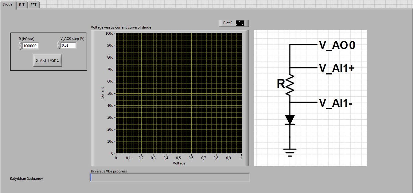
V_AO 0 will generate analog DC voltage which will be increasing by V_AO 0 step which you write in the application. NI myDAQ will read difference between V_AI 1+ and V_AI 1- and divide by R which is our current through diode. Each iteration will be putted on the graph and make curve.
Circuit for analyzing diode characteristics
- Build the circuit as shown in Figure 10. R = 100 kOhm. Silicon diode (1N4001).
- Connect to correct pins of NI myDAQ . Ground to AGND.
- Measure resistor by using digital multimeter.
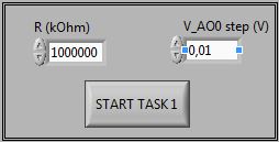
- Open application and write founded value of resistor to R and put 0.1 V for V_AO 0 step
- Run application
- Finally you should have something like this

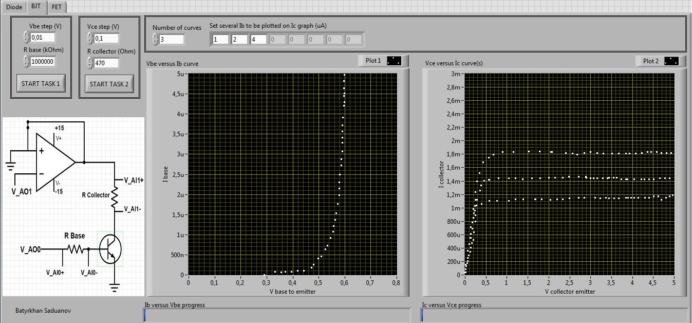
BJT circuit
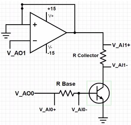
To plot base current (I B ) versus base-emitter voltage (V BE ) graph V_AO0 will be incrementing by steps that written in Vbe step(V). NI myDAQ will read difference between V_AI 0+ and V_AI 0- and divide by R which is our current through base. Each iteration will be putted on the graph and make first curve. For inverting pin of OP AMP analog output voltage(V_AO1) should be connected. For second curve V_AO0 will be set by order written in application and hold while analog output (V_AO1) will be incrementing from 0 V to 10 V by step that you choose by putting Vce step(V). Each iteration will be putted on the graph and make second curve.
- Build the circuit as shown in Figure 11. R base = 1MOhm. R collector = 1kOhm. BJT(2N3904CN).
- Connect to correct pins of NI myDAQ . Supply pins of OP AMP should be connected to +15V and -15V on NI myDAQ. Ground to AGND.
- Measure R base and R collector by using digital multimeter.
- Open application and write founded value of resistors to R base and R collector.
- Put 0.1 V for Vbe step(V) and Vce step(V).
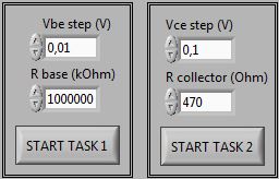
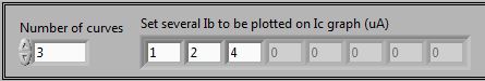
- Write number of curves 3 (you can choose from 1 to 8). Set appropriate three base current (I_B) values into the array.
- Run the application.
- Finally you should have something like this
Application will do same step as in BJT curve tracing. Only difference is that R gate not important (because current through gate equal to 0). You can either pit or remove R gate. To plot drain current (I D ) versus gate to source voltage (V GS ) graph V_AO0 will be incrementing by steps that written in Vgs step(V). NI myDAQ will read difference between V_AI 1+ and V_AI 1- and divide by R drain which is our current through drain. Each iteration will be putted on the graph and make first curve. For inverting pin of OP AMP analog output voltage(V_AO1) should be connected. For second curve V_AO0 will be set by order written in application and hold while analog output (V_AO1) will be incrementing from 0 V to 10 V by step that you choose by putting Vdc step(V). Each iteration will be putted on the graph and make second curve.

FET circuit
- Build the circuit as shown in Figure 11. R collector = 1k. JFET(2N5457).
- Connect to correct pins of NI myDAQ . Supply pins of OP AMP should be connected to +15V and -15V on NI myDAQ. Ground to AGND.
- Measure R drain by using digital multimeter.
- Open application and choose JFET(you can choose from JFET, DMOSFET or EMOSFET ) then write founded value of resistor to R drain.
- Put 0.1 V for Vgs step(V) and Vds step(V).

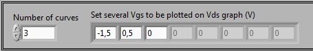
- Write number of curves 3 (you can choose from 1 to 8). Set appropriate three voltage (V GS ) values into the array.
- Run the application.
- Finally you should have something like this

- Repeat same process for DMOSFET and EMOSFET
A diode is a two-terminal element, usually made by using a p-n junction (the operation of which is explained in detail in ROBT204 class). The symbol for a diode is shown in Fig.1 (a). Which terminal is which matters very much in a diode. Usually, the terminal indicated by a horizontal line in Fig. 1 (a), called the cathode, is marked on a real diode; see, for example, Fig. 1(b). We define the voltage (vD) and the current (iD) of a diode as shown in the figure. These two quantities are related, as shown in Fig. 1(c). When the 2 voltage vD is positive, the diode is said to be forward-biased; a large current can then flow, and the diode is said to conduct. When the voltage vD is negative, the diode is said to be reverse-biased; the diode current is extremely small, and for our purposes it is assumed to be zero; the diode is then said to be turned off. Thus, the diode effectively conducts current in only one direction (downward in Fig. 1); it “refuses” to conduct current in the other direction. This property turns out to be very useful, as you will find out in this experiment.

Fig. 1 – Symbolic representation of diodes (a), diode (b), diode IV characteristic (c)
1N4001 diode
Transistors fall into two categories (bipolar junction or bipolar and field-effect) and are also classified according to the semiconductor material employed (commonly silicon, others are germanium, gallium arsenide, etc.) and to their field of application (e.g. general purpose, switching, high frequency, etc.). Various classes of transistor are available according to the application concerned. Bipolar transistors generally comprise NPN or PNP junctions of either silicon (Si) or germanium (Ge) material. (See Figs. 1 and 2). The junctions are produced in a single slice of silicon by diffusing impurities through a photographically reduced mask (in course Integrated Circuit Design). Germanium devices are rarely encountered and are ignored here. Figures 1 and 2, respectfully, show a simplified representation of NPN and PNP transistors together with circuit symbols.
![]()
In either case the electrodes are labelled collector, base and emitter. Note that each junction within the transistor, whether it be collector-base or base-emitter, constitutes a P-N junction.
![]()
Two sets of characteristics are again necessary to describe fully the behavior of the common-emitter configuration: one for the input or base–emitter circuit and one for the output or collector–emitter circuit. Both are shown in Fig. 5. The emitter, collector, and base currents are shown in their actual conventional current direction. Even though the transistor configuration has changed, the current relations developed earlier for the common- base configuration are still applicable. That is, IE = IC + IB and IC = aIE. For the common-emitter configuration the output characteristics are a plot of the output current ( I C ) versus output voltage ( V CE ) for a range of values of input current ( I B ). The input characteristics are a plot of the input current ( I B ) versus the input voltage ( V BE ) for a range of values of output voltage ( V CE ).

JFET’s are of two types, namely N-channel JFETs and P-channel JFETs. Generally N-channel JFETs are more preferred than P-channel. N-channel and P-channel JFETs are shown in the figures below.
![]()
- Source – The terminal through which the majority carriers enter the channel, is called the sourceterminal S and the conventional current entering the channel at S is designated as I g .
- Drain – The terminal, througih which the majority carriers leave the channel, is called the drainterminal D and the conventional current leaving the channel at D is designated as I D . The drain-to- source voltage is called V DS , and is positive if D is more positive than source S
- Gate – There are two internally connected heavily doped impurity regions formed by alloying, by diffusion, or by any other method available to create two P-N junctions. These impurity regions are called the gate G. A voltage V GS is applied between the gate and source in the direction to reverse-bias the P-N junction. Conventional current entering the channel at G is designated as I G .
- Channel – The region between the source and drain, sandwiched between the two gates is called thechannel and the majority carriers move from source to drain through this channel.

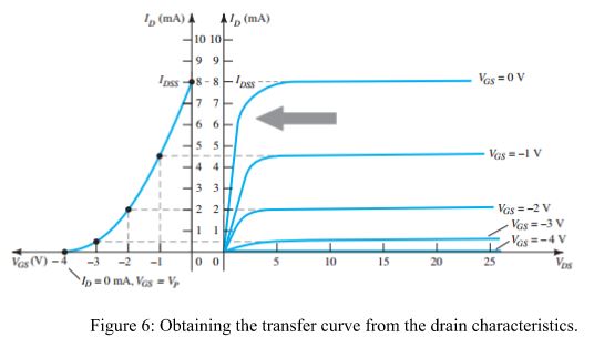
The graphical approach, however, will require a plot of Eq.1 to represent the device and a plot of the network equation relating the same variables. The solution is defined by the point of intersection of the two curves. It is important to keep in mind when applying the graphical approach that the device characteristics will be unaffected by the network in which the device is employed. The network equation may change along with the intersection between the two curves, but the transfer curve defined by Eq. 1 is unaffected. In general, therefore: The transfer characteristics defined by Shockley’s equation are unaffected by the network in which the device is employed.

The transfer curve can be obtained using Shockley’s equation. In Fig. 6 two graphs are provided, with the vertical scaling in milliamperes for each graph. One is a plot of I D versus V DS , whereas the other is I D versus V GS . Using the drain characteristics on the right of the “y” axis, we can draw a horizontal line from the saturation region of the curve denoted V GS 0 V to the I D axis. The resulting current level for both graphs is I DSS . The point of intersection on the I D versus V GS curve will be as shown since the vertical axis is defined as V GS 0 V.
-
JFET-Junction Field Effect Transistor." Electronic Circuits and DiagramElectronics Projects and Design. N.p., 12 Nov. 2013. Web. 03 May 2016. http://www.circuitstoday.com/jfet-junction- field-effect- transistor
-
Boylestad, Robert L., and Louis Nashelsky. Electronic Devices and Circuit Theory. Upper Saddle River, NJ: Prentice Hall, 2014.