Platform Description
In our project we decided to build a universal platform that can be used for different purposes.
This platform feature:
- Display controller
- Expandable ROM and RAM both up 32 KB
- Joystick, Terminal, Keypad Controllers
- Interrupt Arbiter
- Random number generator
- Hex and 7-segment display drivers
- 16-bit Math Coprocessor
- Much more other useful peripheral devices
In this section we will describe hardware part of this platform.
The bare minimum for this platform is Cdm8 CPU, Address Decoder, ROM and RAM
To communicate with devices we need to define what IO bus looks like.
Bus lines:
-
Data- processor data bus -
IO Address- lower 4 bits of processor address bus, generated byAddress decoder -
IO Select- generated byAddress decoder -
Read/Write- processor r/w' signal -
Clock- system clock signal
If we need more program memory we can use ROM controller to get more address space with memory paging technique.
We take Address Out signal of ROM Controller and connect it as higher bits of ROM's address input.

You can read more about ROM Controller here
If we need more RAM we can use similar technique.The difference is that we divide RAM address space into two halfs - lower half is global and upper half is paged.
RAM Controller forms expanded address for RAM chip.
You can read more about it here
In Cdm8 in harvard setup interrupt vectors are located in in upper 16 bytes of program memory and therefore these vectors are constant.
In out platform you can use it as is or connect Dynamic Interrupt Controller which allows you to change these vectors by masking their addresses with external registers.
But this device is unconpatable with ROM controller
ROM Controller takes part in interrupt handling process - when interrupt occurs controller changes memory page to one that is specified on corresponding controller pins.
The easiest way to specify page to handle interrupts is to connect a constant to these pins, however in this case you cannot change it.
Better solution is to connect a register to bus and it's output to ISR Page pins. In that case you can set page dynamically in runtime.
In this block we will describe some devices more precisely.
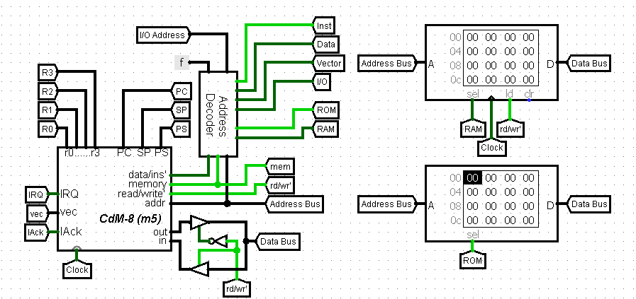
Most of devices connect to IO bus and therefore have similar block and signals that are used to communicate with the bus.
-
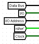
Select- high when someone 'talks' to device, IO selected and IO address is the same as device address.
Of course, address decoding typically implemented through
ANDgates, but there we decided to replace it withlogisim's comparator to have an ability to conviniently set the address of devices. (perf)
-
General bus signals- pins for correspondig bus signals
-
Device data bus- pins that connect to data bus. SignalsWriteandReadare also generated here. They show whether we writing to this device or reading from it.
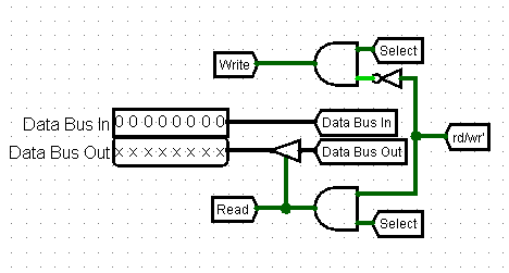
Typically, devices have general singals on their's north side and data bus pins on west side.
The some utility devices.
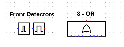
- Front Detectors - two types of regular front detectors with shorter and longer pulse time.
- 8-OR - Fancy 8 input OR gate.
This contoller is used to work with memory banks. It handles bank switching. Moreover it takes part in interrupt handling, when interrupt occurs, controller switches bank to one that specified on ISR Bank input.
When jumping to bank, it saves current bank, it gives ability to jump to bank and then return from it just like regular jsr and rts. Moreover it supports recursive calls.

-
Programmer can switch between banks by writing a number N in range 0x00-0x7F. Then controller will switch to bank N.
-
By writing 0x80 or 0x81 we can return from bank.
-
0x80 is used to return from bank in general.
-
0x81 is used to ruturn from bank and restore registes.
-
If we read from it we get current bank.
To perform a jump you need to specify bank and address in this bank to jump to.
In this example we jump to bank 2 address 0x00:
ldi r0, 0xF0 # Let controller be on address 0xF0
ldi r1, 0x02 # Jump to bank 2
st r0, r1    # Write command to controller
jsr 0x00     # Jump some address in target block
In this example we return from bank:
ldi r0, 0xF0 # Let controller be on address 0xF0
ldi r1, 0x80 # "Return" command
st r0, r1    # Write command to controller
rts          # Return from function
In this example we return from ISR and restore registers:
# Beginning of ISR

pushall      # Save registers

# Some code...

ldi r0, 0xF0 # Let controller be on address 0xF0
ldi r1, 0x81 # "Return and restore" command
st r0, r1    # Write command to controller
popall       # Restore registers
rti          # Return from ISR
(It switches banks by forming high part of address.)

S1 - memory chip that together with counter C1 forms stack, so we can perform push and pop.
R1 - intermediate register that stores byte (command) that was written.
The heart of this device is Sequencer. It is used to execute commands. C2 is a counter that outputs current phase, its output is connected to decoder to convert binary number to separate signal representing phases. D3 - trigger that enables counter.
Delay chain is another important block of this device. It delays the pulse that starts Sequencer by certain amount of clock cycles.
D1 - trigger that indicates that device is handling interrupt.
D2 - trigger that indicates that device is executing some commnd, its /Q output is connected to IR Enable output to disable interrupts while we performing a jump.
How it works....
Executing a command (jump to bank, return):
-
When processor writes a command: command is present in
R1,Write_Clockis high,rti,pop,pushsignals are decoded. -
Write_ClocksetsD2high and so disables interrupts -
Write_Clockstarts aDelay chain, a pulse travels throughDelay chainand then setsD3high and so enablesSequencer. -
Sequencerexecute some commands depending on task and then resets and disables itself and enables interrupts.
Handling an interrupt:
-
When processor starts handling an interrupt,
IAckgoes high. -
IAcksetsD3high enabling sequencer and setsD1high. -
IRswitchesS1data bus toISR Bankinput, setting target bank to bank with ISR's. -
Then, regular 'jump to bank N' command is executed.
Commands:
'jump to bank N':
Command will look like number in range 0x00-0x7F, so general view is 0b0nnnnnnn, where nnnnnnn is target bank number in binary
-
rtiis low,popis low,pushis high -
inc- increnentC1 -
store- writeR1toS1at address inC1 - Then,
0b0nnnnnnnis present onAddress Outand these are higher bits of ROM address
'return from bank':
Command is 0x80 or 0b10000000.
-
rtiis low,popis high,pushis low -
dec- decrementC1 - Then, previous bank number is present on
Address Out
'return from bank and restore registers':
Command is 0x81 or 0b10000001.
- The same as in regular 'return from bank', but
rtiis high. -
rtiswitches multiplexer and sequencer start a couple of clock cycles later. That gives processor time to performpopallinstuction.
All timings in clock-perfect amd were calculated for cdm8 mark 5.
This controller is used to expand RAM.
The first 127 bytes in RAM address space are left as is. Second half becomes paged. We can write to controller to change page, if we read from it we get current page.
-
When we address 0x00-0x7F, we address global part of RAM.
-
When we address 0x80-0xFF, we address one of pages.
This doesn't include IO region. Of course, when we address IO region, we address devices.

The chip takes address bus as input and forms address especially for RAM chip.
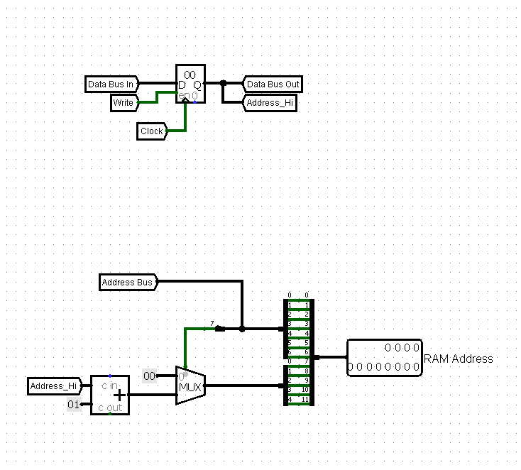
Register here holds current page. Logic at the bottom forms address by taking 7 bits from address bus and adding page bits on top.
If 7-th bit of address bus is zero, that means that address is in range 0x00-0x7F, then we ignore page bits, set upper bits to zero and output a 7-bit address with last bit being zero. This is the case when we address 0x00-0x7F (global part of RAM address space).
When we address paged part of RAM address space, 7-th bit is one, so register content incremented by one goes to upper bits of address.
This device handles 8 separate prioritized interrupts.

It connects to processor IRQ, vec and IAck pins.
On south size it has pairs of INTn and IAckn pins.
They are arranged like this (from left to right):
INT0, IA0, INT1, IA1, ... , INT7, IA7
Where INTn is request line for interrupt with vector n and IAn is corresponding IAck pin.
INT0 has the highest priority, INT7 - the lowest.

Thiggers D0-D7 store current state of interrupt request lines.
- 1 means that interrupt is requested
- 0 means that interrupt is not requested
These triggers are set to 1 asynchronously when high state is present on consequent INT pin.
When some trigger goes to 0 that means that this interrupt is being handled by processor and then consequent IA pin pulses.
D8 is a buffer for processor IRQ signal.
If there are no active requests at the moment and one of INTn pins is high then n is latched to R1 as interrupt vector, D8 goes high requesting processor to handle interrupt with vector n.
If there are some active requests at the moment then on falling edge of processor's Iack the leftmost trigger with high state is reset and number of next trigger with high state is latched into R1 as interrupt vector and then processor IRQ line is retriggered. This defines interrupt prioritization.
This device is addon to Interrupt Arbiter that gives ability to disable certain interrupts.
We can write a byte to it to set new state. If we read from it we get current interrupt state.
Bits in this byte enable or disable certain interrupts:
-
Bit 0 corresponds to INT0
-
Bit 7 corresponds to INT7
-
If bit is one - interrupt is enabled
-
if bit is zero - interrupt is disabled

It connects to Interrupt Arbiter from north and has IRQn and IAckn pin pairs on south side just like Interrupt Arbiter.

Inside it is basically a register. Its bits are ANDed with corresponding IRQ pins.
Device has Enable pin that disables all interrupts. It is raised to 8 bits and ANDed to register bits.
IAckn signals just go through it.
This device forms signals that represent what memory region processor currently addressing.

Beside connecting to processor, you need to specify where would IO region be. If we connect it like on picture, we get IO to be on addresses 0x70-0x7F.
Output signals:
-
Inst- instruction region -
Data- data region -
Vector- interrupt vector region -
I/O- IO region -
ROM- ROM chip select -
RAM- RAM chip select -
IO Address- IO deviecs address for IO bus

-
ROMis high, when eitherInstis high orVectoris high - both instuction and vector are in ROM. -
IO Addressis lower 4 bits of address bus. -
Other signals are formed in a obvious way.
| data/ins' | Offset = IO Offset | Offset = 0xF | Decoder Output |
|---|---|---|---|
| 0 | 0 | 0 | Inst |
| 0 | 0 | 1 | Vector |
| 0 | 1 | 0 | Inst |
| 0 | 1 | 1 | Vector |
| 1 | 0 | 0 | Data |
| 1 | 0 | 1 | Data |
| 1 | 1 | 0 | I/O |
| 1 | 1 | 1 | I/O |
This controller is used when you need dynamic interrupts vectors without using ROM controller.
However, this controller has very limited scope and that's why it won't be described here.

This device is simple 8-bit register connected to I/O bus.
You can write to it and read from it.

This device is a couple of registers arranged in stack configuration. Size of this stack is 20 bytes.
If you write to it, you push a value. If you read from it, you pop a value.
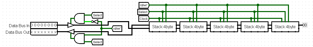
Where each Stack 4 byte is:

This device is used to drive two hex displays.
It is similar to regular IO Register, but has special interface for two hex displays. Contents of registed are displayed.

This device is similar to previous one, but it has special interface for 7-segment display.

This device connects logisim's stock random number generator to IO Bus

We can read 8-bit random number. After reading a new number is generated.

This controller is used to drive logisim's 32x32 pixel LED matrix (mode 3 - "Select Rows/Columns").
It has monochrome and color versions.

We can write bytes to it and thus send data or commands. If we read from it, we get last command or data written.
Available commands:
- Write a pixel at (X, Y)
- Write a block of pixels at (X, Y)
- Clear screen and then write a pixel at (X, Y)
- Clear screen and then write a block of pixels at (X, Y)
- Clear screen
You can send either a data byte or a command byte.
Data byte looks like this: 0b0ddddddd
-
Its most significant bit is zero, it indicates that it is data byte.
-
ddddddd- 7-bit data word (X, Y, Pattern/Mask).
Command byte looks like this: 0b1lwcxbgr
-
Its most significat bit is one, it indicates that it is command byte.
-
l- block, if zero - print single pixel, if one - block of pixels. -
w- write, if zero - don't print anything, if one - print something. -
c- clear, if zero - don't clear screen, if one - clear screen before other actions. -
x- not used -
b- blue component -
g- green component -
r- red component
Color components are 1-bit so we get 3-bit color and thus we can have up to 8 colors (black is also a color, it is coded 0b00000000).
In monochrome mode only r component is used, it defines whether pixel is on or off.
Command examples:
-
0b10010000- clear screen -
0b10100001- write red pixel -
0b11100010- write block of green pixels -
0b10110100- clear display and then write blue pixel -
0b11110001- clear display and then write block of red pixels
How to send commands:
-
To perform clear command we just send one byte with command itself.
-
To perform single pixel write commands (including ones with clear) we need to send three bytes: first byte is
X, second byte isY, third byte is command itself. -
To perform block pixel write commands (including ones with clear) we need to send four bytes: first byte is
mask, second byte isX, third byte isY, fourh byte is command itself.
(0, 0) is in the lower left corner
Code samples:
In this example we print green pixel at (10, 15):
ldi r0, 10          # X
ldi r1, 15          # Y
ldi r2, 0xF6        # Controller address
ldi r3, 0b10100010  # Print green pixel command

st r2, r0           # Write X
st r2, r1           # Write Y
st r2, r3 # Write Command![]()
In this example we clear screen and then print block of red pixels at (6, 5):
ldi r0, 6           # X
ldi r1, 5           # Y
ldi r2, 0xF6        # Controller address
ldi r3, 0x55        # Mask (0b01010101)

st r2, r3           # Write Mask
st r2, r0           # Write X
st r2, r1           # Write Y

ldi r3, 0b11110001  # Clear screen and print
                      a block of green pixels

st r2, r3 # Write Command![]()
![]()
In this example we simply clear screen:
ldi r2, 0xF6        # Controller address
ldi r3, 0b10010000  # Clear screen command

st r2, r3           # Write command
Now we will focus on monochrome version. More about displaying color later.
This controller is designed to be used with LED matrix in mode 3 ("Select Rows/Columns"). In this mode matrix has two inputs on west side. Upper is column select and lower is data. You can read more about matrix behaviour in this mode in the official documentation
So, controller has the same two outputs which you connect to the matrix.
Controller generantes scan signal - pulses bits one by one on Scan pin and simultaneously outputs approrpiate data on Data pin. Repeatedly going through all 32 colomns, we get an image.
To be able to write to display without graphical artifacts (we can't read from memory and write to it simultaneously, if we want to write something to chip, it can't outupt data to matrix, thus we get an artifact on screen), we use two buffers - active, data from it goes to output, and shadow buffer - we write new data to it. Buffers store 32 32-bit words, each word corresponds to one colomn. Buffers must store identical data.
When we update state of buffer:
- Data is written to shadow buffer
- Buffers are swapped, changes are now displayed
- The same data is written to the second buffer to keep the same data in buffers.

C1 is main counter, counts colomns to 32, connected to col signal.
In Scanline Generator we pass col through decoder and then wire its output to one 32-bit word to get scan signal. The delay chain here is needed to fix timings.
M1 and M2 are video buffers.
D1 is trigger that chooses active buffer (other would be shadow buffer). It is wired in a flip-flop configuration, so on clock it switches its state and thus changes active buffer.
Memory Multiplexing Logic consists of different demultiplexors and multiplexors that wire M1 and M2 in a correct way (active buffer is wired to output, shadow buffer is wired to internal scheme).
Append Logic is used to get a 32-bit word from buffer, modify it, and then write it back to buffer. It just modifies bitword through ANDing or ORing this bitword with some bitmasks. Depending on command, bitmask can be either one bit (to write single pixel) or 7-bit (to write block of pixels). These bitmasks are generated by this logic in obvious way.
Data Queue is four registers arranged in a queue. This queue is used to store commands and data. When we write a byte, it goes to the first register and all other registes are pushed forward. When we read, we get contents of the last register. Registers are wired to these signals (from left to right): cmd, y, x, mask. This defines data prococol that we described before.
Command Decoder is used to decode controls signals and color data from command byte.
Finally, Sequencer is used to sequently execute some internal commands (clear, write to buffer, swap buffers). D2 is its Count Enable trigger and C2 is counter itself.
How it works....
-
When a byte is written,
writesignal pulses. -
writeresetsC2and enablesD2 -
If there is no command present (data byte was written) then
D2is set low, sequencer doesn't do anything, scheme waits for next byte. Otherwise,Sequencermakes its cycle and then resetsD2and thus stops itself.
Then, there are four phases:
- On phase 0, we clear both
M1andM2ifclearcommand is decoded. - On phase 1, we write to shadow buffer, if
writecommand is decoded. - On phase 2, we swap buffers.
- On phase 3, we write to other buffer, if
writecommand is decoded.
When we write to one of the memory chips, data from its output goes through Append Logic and then back to its input. By doing that we modify bitwords in memory chips.
Displaying color:
When using monochrome version of controller, we simply connect one matrix to its outputs.
We can display different colors by stacking a bunch of martices on top of each other. The key thing here is to set their colors to red, green and blue, but with opacity not equal to 255 (in our case we picked opacity for each matrix to be 255/3). In that case we allow matrices to blend their color and thus get an ability to diplay multiple colors at once.
In fact, we can't directly stack matrices on top of each other, that's why we introduce some offset to it (1 pixel).
Proper way of stacking martices is shown on picture below:
![]()
Because of offset, active zone of screen loses 2 pixels, thus resolution of screen in color mode is 30x32 pixels, in monochrome mode it is 32x32 pixels.
This controller drives 4-bit joystick.

Additional pins:
- X,Y (west) - pins to X and Y outputs of joystick

It just connects 4-bit X and Y pins to data bus.
When reading from it you get actual position of joystick.
This controller can drive up to 8 buttons. It can be used in polling mode or through interrupts.

Additional pins:
- IRQ (north) - interrupt request line for this device, active when some buttons are pressed
- Button pins (south) - 8 pins for buttons
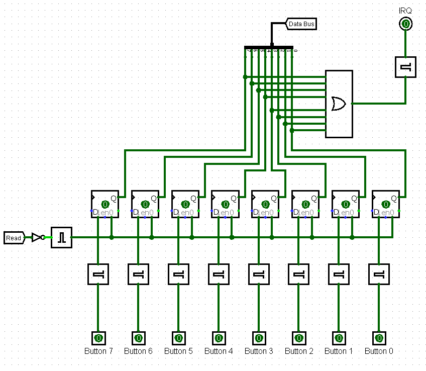
It has 8 D-triggers each connected to a bit in a data bus. Buttons asynchronously set corresponding triggers. Triggers are reset on falling edge of Read signal (which is rd/wr' AND Select).
So, when reading from it, processor gets a byte that contains information about buttons that were pressed in the past (If some bit is 1, then corresponding button was pressed). After reading, all triggers are reset.
Moreover, if all triggers were zero and some button is pressed then a pulse occurs at IRQ output triggering interrupt.
This controller is used to drive terminal and keyboard.
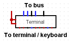
Additional pins:
- Terminal/Keyboard pins (south) - pins that connect to terminal and keyboard

This controller basically just connects terminal and keyboard to bus in a way that when writing, 7 bits of data (as ASCII symbol) goes to the terminal and last bit of data AND Write forms Terminal Clear signal. That means that we can write a character to terminal as well as clear it by sending 0x80.
When reading keyboard buffer connects to 7 bits of data bus and Keyboard Available goes to the last bit of data bus. That helps to read out a whole buffer. Just read from this device while data is not equal to 0x80.
This device supports interrupts. If keybaord buffer was empty and then there was some input, a pulse occurs on IRQ.
In this part we will describe software part of this platform.
As we use more than 256 bytes of program memory and need to work with a lot of code. Default development tool (CocoIDE) is very uncomfortable to use when working with multifile projects and that's why we developed some tools to make software development process easier.
The main application that does hard work is cocomake. It is an incremental build system designed to work with big multifile projects.
It is incremental, so only modified files get recompiled. That makes compiling much faster.

There, only battleship_arbiter.asm got recompiled as other files were not modified.
You can define a toolchain - set programs which will be applied to file.
Each file is compiled with this toolchain to an 256 byte image and then these 256 byte images glued together to produce one big image that you load straight in logisim.
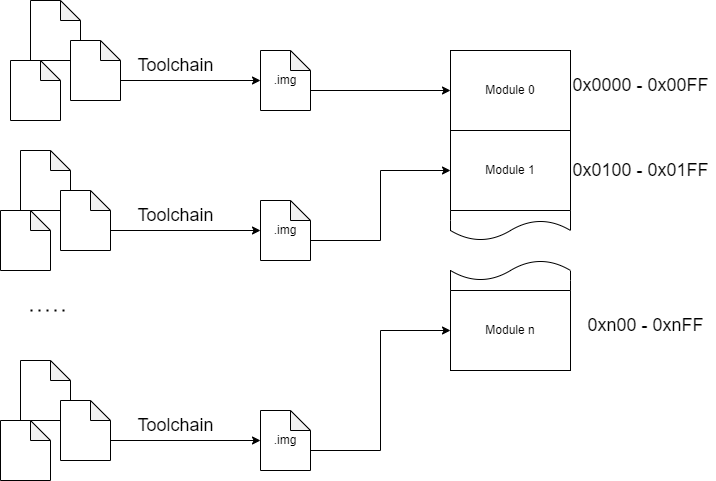
So, you can have one big project with a lot of files spannig to many modules and you just execute one command and get your project compiled in one image.
More about cocomake here
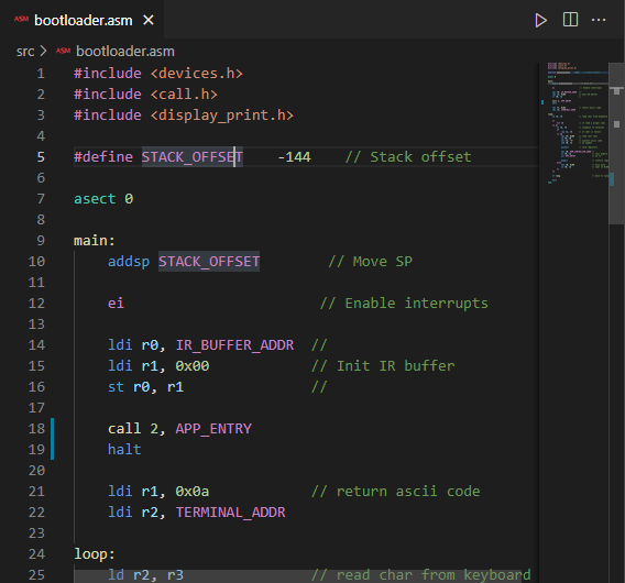
For the text editor we decided to use VS Code as it is free modern software with a lot of customization options via extensions.
To make support for cdm8 assembler we developed an extension for VS Code that adds syntax highlighting for assembly and C preprocessor directives as well as code snippets.
This extension is published in VS Code Marketplace can be easily found.

Extension page in VS Code Marketplace
There is an example how the code looks with this extension:
In this section we will describe our demonstration setup.
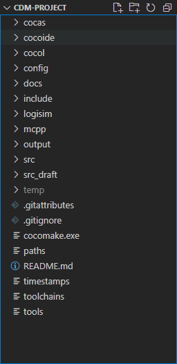
So, full project tree looks like this:
Let's take a look on cocomake configuration.
In paths file we define relative paths to working folders:
src=src
temp=temp
output=output
There we set source files folder to be src/, temporary files folder to temp/ and folder where final images would be to output/.
In tools file we define all the tools that we will use in our toolchain. These are assembler cocas, linker cocol and C preprocessor mcpp:
cocas=python cocas\cocas.py->obj
cocol=python cocol\cocol.py->img
mcpp=mcpp\mcpp.bat->asm->_p
debug=python cocoide\cocoideV1.91.pyw
The debug application is also defined here. It is set to CocoIDE, so when we run cocomake -d [file], it will open this file in CocoIDE for debug.
Next, we define toolchains themself in toolchains file:
asm=mcpp->cocas->cocol
obj=cocol
img=
There we configuring build system to pass .asm files through mcpp, cocas, cocol and then link to final image, pass .obj files through cocol and then link to final image and link .img files directly to image.
Then, we can create some .cocomake files that would describe final images, these are located in config directory.
For example we have firmware.cocomake:
firmware.img
0:bootloader.asm
2:display_print.asm
5:app_example.asm
If we run cocomake config/firmware.cocomake, we will get firmware.img in output directory as result.
Memory map of this image would look like this:
0000-00FF: bootloader.asm
0100-01FF: -
0200-02FF: display_print.asm
0300-03FF: -
0400-04FF: -
0500-05FF: app_example.asm
Our demonstration config is battleship.cocomake. To build it run cocomake config/battleship.cocomake.
As you might have noticed, we use mcpp in our toolchain. That's because cocas doesn't have any include functionality. For multifile projects this feature is critical.
So, source files are located in src directory and header files are located in include directory.
For example, in devices.h file we define all devices' addresses and so we can use this header in other files.
#include <devices.h>

// ...

ldi r0, IR_BUFFER_ADDR  //
ldi r1, 0x00            // Init IR buffer
st r0, r1               //

// ...
There, IR_BUFFER_ADDR is from devices.h.
Another important application of headers is libraries. We can put some macros and rsects in header file to form a library.
For example, we have call.h which defines macros to work with modules and ROM Controller.
#include <call.h>

// ...

call 5, DEFAULT_ENTRY

//...
There, call is macro for calling other module defined in call.h, DEFAULT_ENTRY also defined in call.h and stands for module default entry point (0x00).
Moreover headers can be used to export entry points for a module.
Logisim schemes are located in logisim directory.
The main file is cdm-platform.circ. It contains only one scheme - one that we use for demonstration.
This file imports cdm8 scheme and CdM8_mb5_library which has all the devices.
So, in cdm-platform.circ we just connect CPU and all the devices with wires.
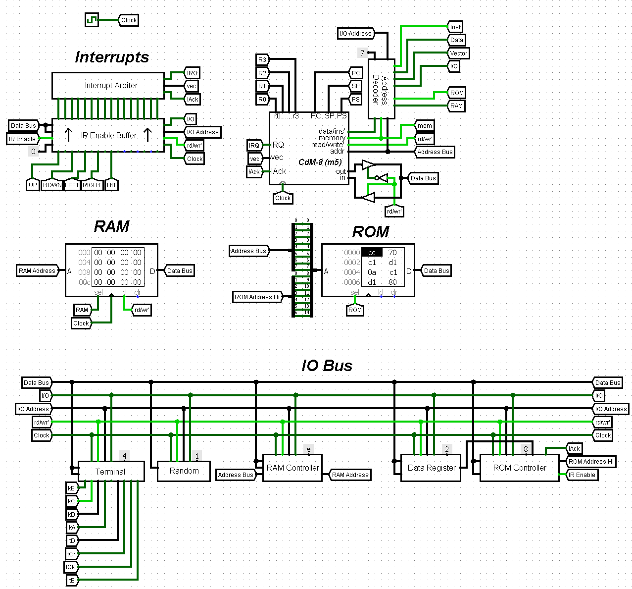
Here we have:
- Cdm8 mk5 CPU
-
Address Decoderwith a0x7constant, that means devices will be on addresses0x70-0x7F -
Interrupt ArbiterwithIR Enable Buffer - RAM and ROM
- IO Bus with a lot of devices
Devices on IO Bus:
- Terminal Controller
- Random Number Generator
- RAM Controller
- ROM Controller with a register attached to
ISR Pagepin
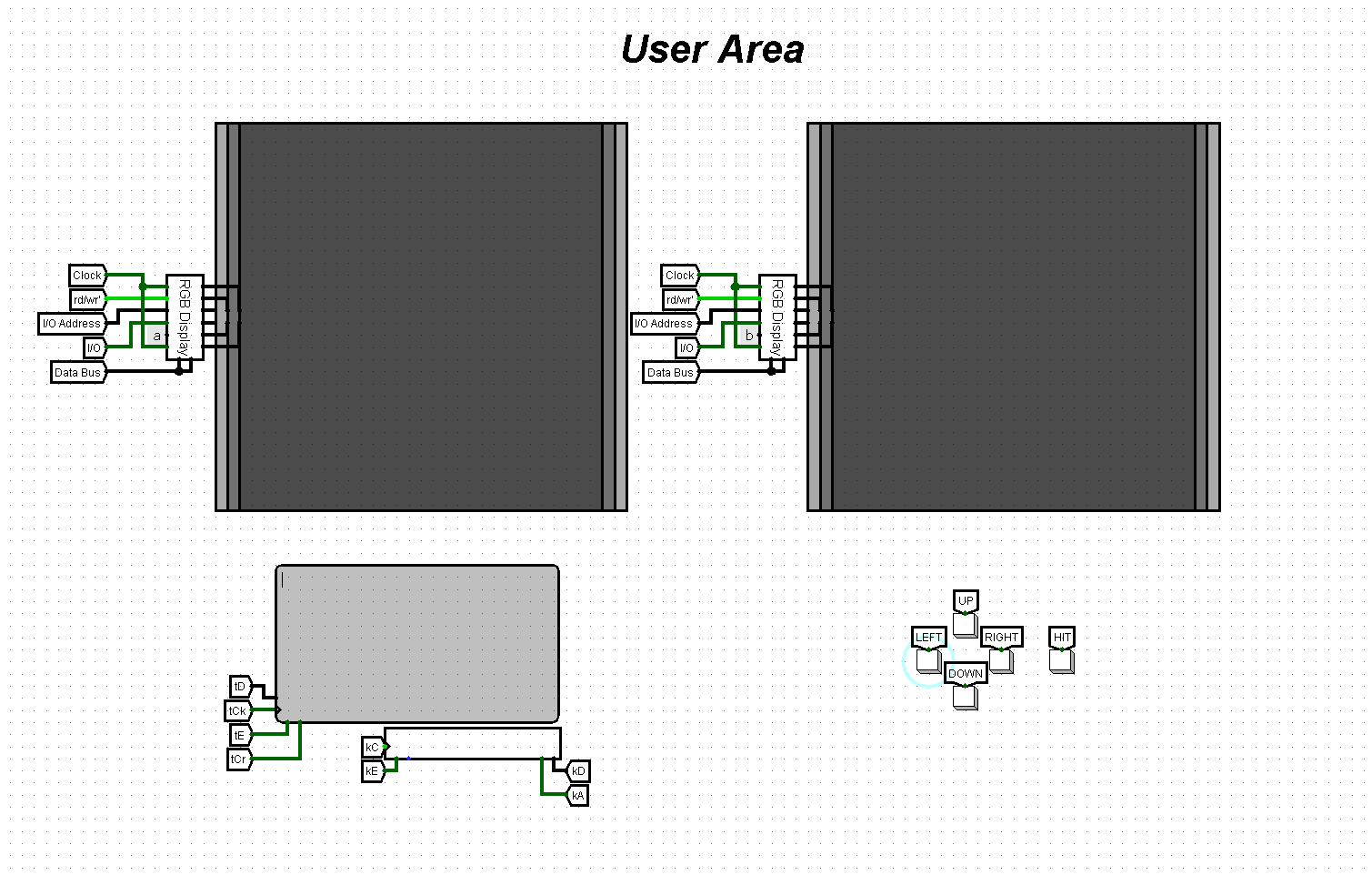
In user area we have:
- Two 8 color 32x32 screens connected to display controllers
- Terminal connected to terminal controller
- Buttons connected to
INT0-INT4
Buttons are connected to individual interrupts to speed up their processing. This way, we skip decoding state of each button from byte (if we use keypad controller, for example) and just put code for each button as ISR.
RAM Layout:
-
0x00-0x6F- stack and global variables memory -
0x70-0x7F- I/O devices -
0x80-0xFF- paged memory
So, our demonstration firmware consists of bootloader, some libraries, sample program that prints "Hello world!" and our main application - Battleship game.
Image (battleship.img) memory map looks like this:
0000-00FF: bootloader.asm
0100-01FF: display_print.asm
0200-02FF: app_example.asm
0300-03FF: battleship_isr.asm
0400-04FF: battleship_main.asm
0500-05FF: battleship_draw_map.asm
0600-06FF: battleship_arbiter.asm
0700-07FF: battleship_computers_turn_0.asm
...
0B00-0BFF: battleship_computers_turn_4.asm
0C00-0CFF: battleship_players_turn.asm
0D00-0DFF: battleship_print_killed_ship_1.asm
0E00-0EFF: battleship_print_killed_ship_2.asm
...
6400-64FF: battleship_map0.asm
6500-65FF: battleship_map1.asm
...
7200-72FF: battleship_map14.asm
7300-73FF: battleship_map15.asm
Battleship
To show the capabilities of our platform we decided to code Battleship game (soviet/russian varitant).
Rules are standard for this variant of game. In our version player plays against AI.
Gameplay:
When you start a program, it loads random maps to RAM and draws player's map on screen. After that game begins.
- Player's field is displayed on left screen
- Enemy's field is displayed in right screen
- A line at the top of the screen shows whose turn is it.
Player has cursor on his screen which can be moved with buttons (left, right, up, down). Hit button fires a shot.
Logic of the game looks like this:

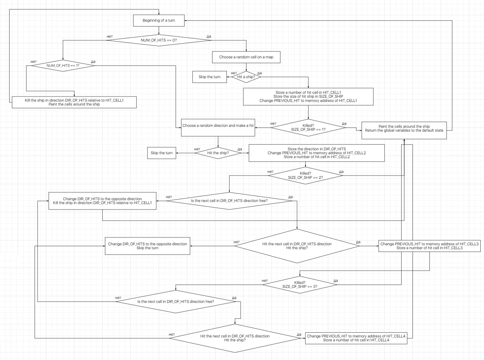
We implemented quite clever AI:
However, game some limitations:
- Maps for AI, and for player are hardcoded (16 maps) and randomly picked on start.
- If a player kills a part of the ship, he/she must continue to kill exactly this ship (standard tactic).
In all other aspects it is fully functional battleship.