Hardware Design

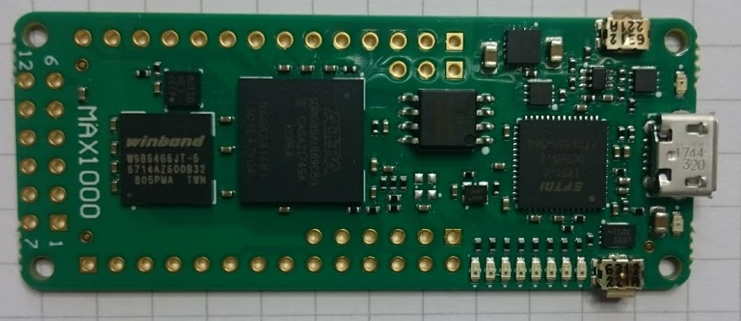
The heart of the radio is the MAX1000 FPGA module. This contains a small, yet quite capable MAX10 FPGA made by intel (used to be Altera). To make the design simple, and as cheap as possible I have tried to put as many features as possible into the FPGA.
- The FPGA implements all the SDR functions, (de)modulation, filtering, AGC, audio processing. CW, SSB, AM, and FM modes are implemented.
- The built-in 12-bit ADC digitises the microphone input, the battery level indicator, and the forward and reverse power inputs from the SWR bridge.
- The speaker output is generated by a 1-bit sigma-delta DAC implemented in FPGA logic.
- A 1MHz, 12-bit PWM output modulates the switch-mode RF power amplifier.
- The local oscillator is implemented using a numerically controlled oscillator in FPGA logic.
- The FPGA contains a small CPU to drive the user interface.
- The FPGA provides a GPS 1-PPS input for precise frequency calibration.
- The FPGA provides a signal generator output for self-test.
The user interface is a simple and functional design using a rotary encoder for tuning and menu navigation, along with four tactile switches. The display is an inexpensive 16x2 character LCD. An i2c EEPROM provides storage for calibration data and up to 500 memories.
Provision is made for a built-in microphone and speaker, while 3.5mm jacks are provided for microphone and headphones. This allows inexpensive PC/multimedia devices to be used out of the box. A Push To Talk switch can also be connected to the microphone jack. A separate jack allows a straight or iambic telegraph key to be connected. The FPGA provides digital control of volume and microphone levels, removing components to help keep costs down.
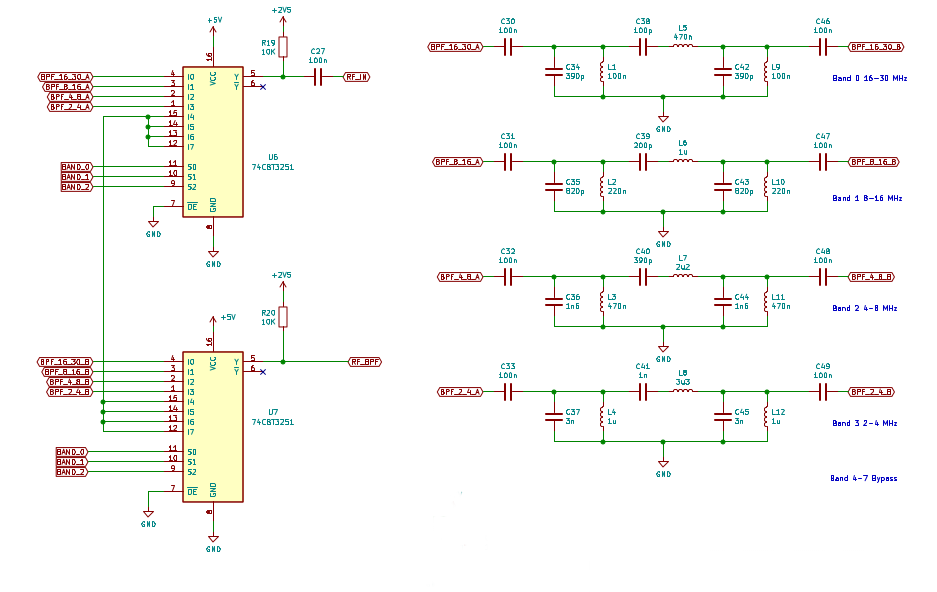
The Quadrature Sampling Detector (QSD) mixer uses a square wave local oscillator and is therefore sensitive not only to the tuned frequency but also to odd harmonics, the strongest being the third harmonic (3x the tuned frequency). To prevent signals at the harmonic frequencies interfering with the signal of interest, a band-pass filter is placed in front of the receiver.
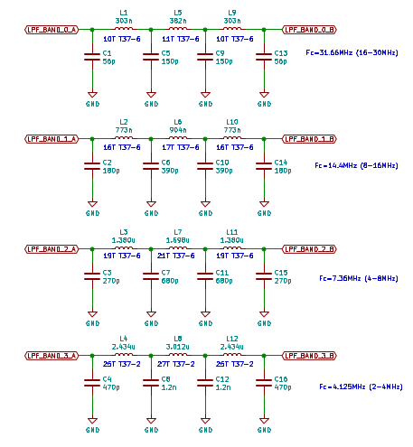
The entire HF spectrum is broken down into several bands each with a separate band-pass filter. To prevent the third (and higher harmonics) from being received, the high cut-off frequency must not be greater than the 3x the lower cut-off frequency. In the real world, filters roll off slowly, so we ideally to allow some extra margin say 2x the lower cut-off frequency.
Using this approach, we can cover the whole HF spectrum from 3MHz to 30MHz with only four filters.
| Band | f1 (MHz) | f2 (MHz) |
|---|---|---|
| 0 | 16 | 30 |
| 1 | 8 | 16 |
| 2 | 4 | 8 |
| 3 | 2 | 4 |
This technique is used in both the soft-rock (ensemble) and mcHF designs (among others), using an analogue multiplexer to switch between bands. The QRP-labs design uses much narrower plug-in BPF modules which each pass on of the HF ham bands. The QRP-labs design does a better job of filtering out unwanted signals outside the ham bands, but a filter is needed for each band (which would be a lot of filters). The OpenXcvr design uses a 4 band filter to reduce cost, and allow a general coverage design that could also be used for Short Wave Listening (SWLing).
In common with the mcHF design, wire-wound surface mount inductors are used. The surface mount inductors reduce cost and board area but still provide a reasonably high Q factor. The 2MHz lower frequency limit of band 3 will probably allow reasonable performance on the 1.8MHz (160m) band, due to the slow roll-off of the filter. To allow maximum flexibility, e.g. for commercial broadcast on LW and MW bands, a bypass option is also included.
The resistor and inductor values were calculated using an online calculator. The filters are all 3rd order Chebyshev designs, the surface mount inductors are only available in a limited range of values, so the E6 range was chosen. The impedance of both the input and output impedance is 50 ohms.
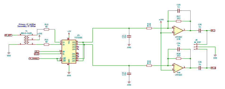
There a few variations on the basic design that have been used in previous projects. The soft-rock receivers use a transformer to create positive and negative versions of the signal, and the analogue switch passes either the positive or negative signal to a single-ended amplifier to achieve a mixing effect. The QRP-kits also uses a transformer to create a positive and negative version of the input signal, but both positive and negative versions of the signal are passed to a differential (instrumentation) amplifier.
In the early prototypes, a differential amplifier was used to eliminate the hand-wound transformer, but this required 3 dual op-amps which increased the cost. I have now switched to a transformer-based approach, using a single-ended amplifier, which only requires one dual op-amp IC. A prototype showed very similar performance between the two designs.
The soft-rock uses an LT6231 op-amp, whereas the QRP-labs design uses an LM4562 op-amp. The LT6236 has better noise performance than the LM4562 but is more expensive. The prototype receiver used a QRP-labs receiver and this gave very good results. For this reason, the less expensive LM4562 was chosen, but using an 8-pin SOIC package rather than a DIP package. The 2 devices are footprint compatible so it should be possible to substitute either device (although I haven't tried this).
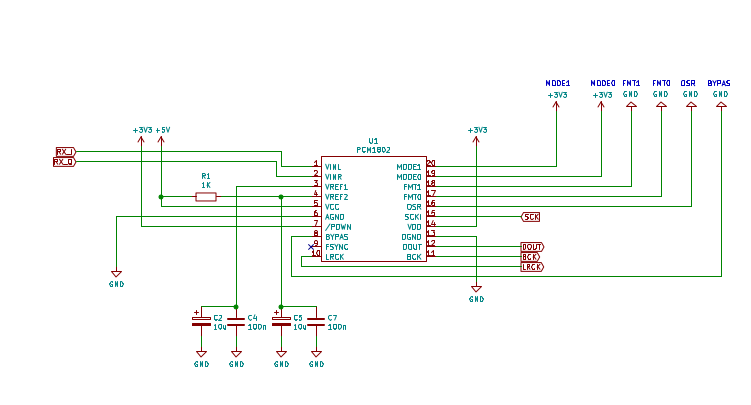
The MAX 10 device has an in-built 12-bit ADC, I did some experiments using the inbuilt ADC, but I didn't get very good results. I think that the 12-bit ADC just doesn't have sufficient dynamic range for this application. I considered using a programmable gain amplifier to drive the ADC but rejected this idea because it would be more expensive than using a dedicated audio ADC and would not have performed as well. Many modules using a 24-bit stereo PCM1802 ADC are available cheaply on eBay, one of these modules was selected for the prototype and it worked well. These ADCs are inexpensive and provide more than adequate dynamic range. They also allow a decent sample rate of 96kS/s providing more than enough bandwidth for the modes used on HF ham bands.
The FPGA processes the I/Q signals provided by the PCM1802 ADC, producing a mono audio signal. This signal needs to be converted into an analogue signal to drive the headphones/speakers. This DAC doesn't need to be Hi-Fi grade, the audio output of the radio only has a limited dynamic range and bandwidth (3KHz is enough to reproduce intelligible speech). A sigma-delta modulator allows a DAC to be constructed using a single FPGA GPIO pin, followed by a simple RC filter with a cut-off frequency of ~3KHz. The sigma-delta DAC works on the principle that bandwidth can be traded for an improved signal to noise ratio (SNR). In this case, the GPIO pin is toggled at a rate of 150MHz while the highest frequency of interest is only 3KHz, this gives an oversampling ratio of 25000. Ordinarily, an extra bits-worth of SNR is gained each time the sample rate is multiplied by 4, in this case giving about 7 bits. A sigma-delta modulator provides noise shaping, this moves the majority of the quantisation noise out of the band of interest, where it is removed by the filter. For a first-order sigma-delta modulator, we get approximately twice as many bits for the same oversampling ratio. This is equivalent to ~14 bits, which is plenty.
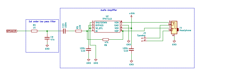
The sigma-delta ADC provides enough dynamic range to allow digital volume control to be implemented in the FPGA, reducing the parts count and cost. The prototype audio amplifier uses an LM386, with the minimum gain of 20x. Since the gain was more than necessary, a trim pot was used to set the maximum attenuation. To reduce the cost, a more modern and very inexpensive TPA711D replaced it. The TPA711D is configured to have a fixed gain of x10, also removing the cost of the trim-pot. A low-pass RC filter removes the switching noise introduced by the sigma-delta DAC.
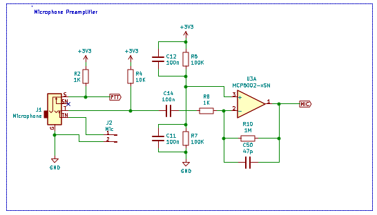
The first prototype design used a max9814 based module with an electret condenser microphone. The max9814 gave enough gain to drive the 0-3v input of the FPGAs built-in ADC, and the inbuilt AGC also worked well. The AGC also has the effect of amplifying background noise, which isn't desirable for a communications transmitter. For this reason, it was decided to use a simple operation amplifier with a fixed gain of 60dB. The FPGA has sufficient capacity to provide any gain control/compression that might be needed. The amplifier uses a very cheap MCP6002 dual op-amp. The other half of the amplifier is used to generate a 2.5v split supply rail to bias signals in the FST3253 bus switches.
The OpenXCVR is designed to have a low-cost yet efficient QRP-level power amplifier. A simple and efficient design reduces the cost and allows for portable battery-powered operation.
The RF power amplifier draws upon a number of CW transmitters that use the BS170 n-channel MOSFET in a switching configuration to achieve a very high efficiency. These designs by KD1JV, the norcal 2030, this design by kk9jef and the QCX+ all use similar designs to give 5W(ish) with a 12v supply.
Some background info on these types of design can be found in these articles. The main drawback of this kind of amplifier is that the output is non-linear, in an ideal amplifier the transistors would always be fully-on or fully-off. This is fine for modes with a constant envelope such as CW or FM, but it won't work for AM or SSB.
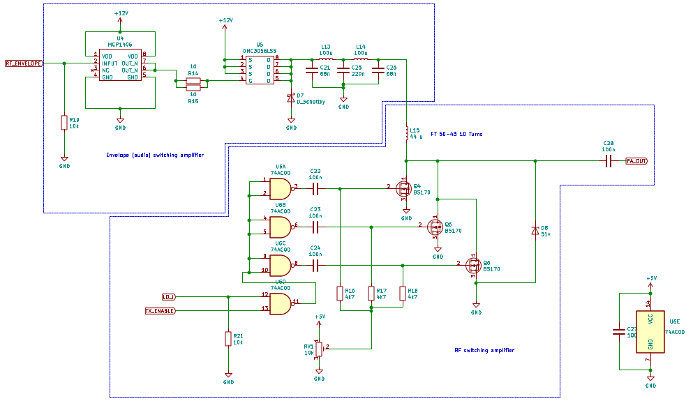
These lecture notes describe how the power supply can be varied to control the amplitude of the RF output. An innovative modification to the QCX puts this technique into practice. This type of amplifier turns out to be a very good fit for this project and results in simpler firmware and hardware. In this scheme, the RF amplifier is the transmit mixer.
The baseband signal is present in the transmitter in a rectangular (I and Q) form. This can be converted into polar (phase and magnitude) form using the CORDIC algorithm. (This is a component that already exists in the receiver firmware). The phase component is simply added to the accumulator in the NCO, modulating the phase of the local oscillator. The local oscillator becomes the RF signal that is amplified by the switching RF amplifier. The magnitude component controls the supply voltage to the RF amplifier. This is achieved using an audio amplifier. Since the RF Amplifier is so efficient, it would be a shame to waste power in the audio amplifier. An efficient amplifier capable of supplying more than 5W of audio power is required.
The OpenXcvr uses a class-D amplifier. The PWM amplitude signal from the FPGA switches a single p-channel MOSFET. A Schottky diode allows current to flow through the output filter inductors while the FET is switched off. The circuit is identical to a buck converter, but it is more useful to think of the circuit as an amplifier because the voltage level is changing while the load remains constant. A 5 pole LC filter removes the amplifiers switching noise.
The BS170 transistors forming the RF power amplifier are driven by 74AC series logic that has a 25mA drive strength. To allow the maximum drive to each transistor, each transistor is driven by a separate logic gate. The fourth gate conveniently switches off the amplifier when in receive. To help ensure that the transistors get switched completely on, a trimmer potentiometer provides a variable "bias". Note that the transistors should be off when the drivers are inactive, so the bias voltage is adjusted just below the threshold voltage say 3v. The MOSFET gates can then swing from about around 3-8v. Many similar designs are class-E designs (or "resonate out" the drain-source capacitance) to achieve greater efficiency. This approach limits the bandwidth of the amplifier. Since I want to operate across a range of HF bands, I have decided not to adopt this approach. In practice, the source-drain capacitance of the BS170 is actually relatively low, so the power loss due to this capacitance is quite low compared to the other losses.
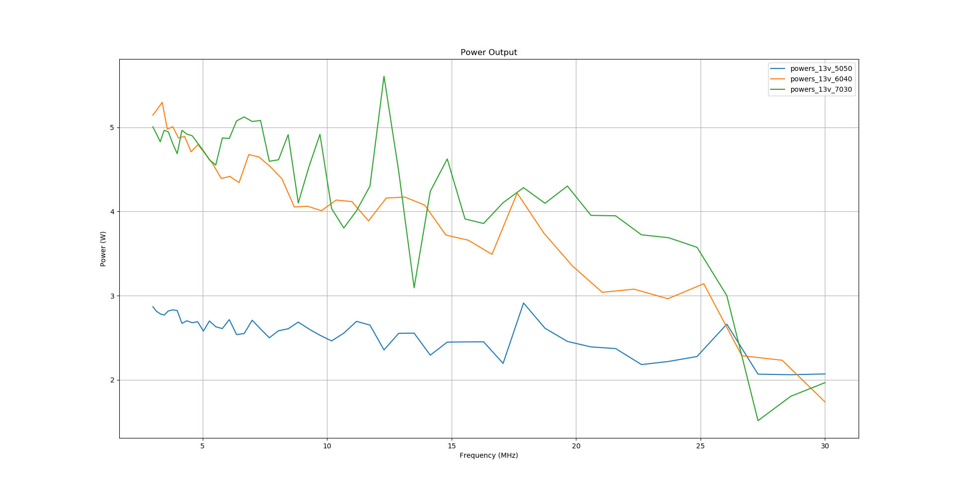
The flexibility of the FPGA allows some other properties of the switching amplifier to be exploited. It is fairly easy to increase the duty cycle of the local oscillator, which in turn increases the voltage swing of the RF output. Some experiments have shown that higher duty cycles increase power output. These changes in duty cycle have a similar effect to increasing the turns ratio of an output transformer, giving an improved match between the amplifier and the load. Control of the duty cycle allows the firmware to tweak the amplifiers output impedance, without any additional expense.
The Power Amplifier is a non-linear design, which creates harmonics, good practice dictates that a low pass filter should be employed after the Power Amplifier to prevent unintended emissions.
The low pass filter must handle 5 (ish) watts of RF power, so the inductors used in the low pass filter are hand-wound toroidal inductors. OpenXCVR uses a relay switched design similar in principle to mcHF and ubitx. This article provides the basic filter designs.
AXICOM d2n relays have been selected because they have been used successfully in other HF applications for example in ubitx and easy tr switch.
The transmit-receive switch simply uses an AXICOM d2n relay to switch the antenna connector between the RF input to the receiver and the RF output from the Power amplifier. A BS170 MOSFET provides the active-low transmit enable signal used by the QRP-labs power amplifier to switch off the bias voltage when receiving.
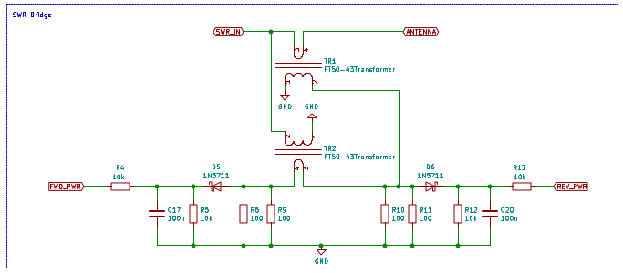
This article describes the design of a QRP SWR meter using an Arduino and a Stockton Bridge. OpenXCVR uses the same basic design but uses spare FPGA analogue inputs to measure the forward and reverse power.