This repository has been archived by the owner on Sep 12, 2020. It is now read-only.
Quirks of PCB manufacturing at ITead
I do all my PCB production at ITead Studio the price is low and their published specs are nice, but there are some quirks that you need to be aware of to get good product.
- Don't go to the absolute limits with everything, I use 8 mil clearance/width by default and go down to 6 mil only where needed, this gives a more error-tolerant design.
- Make sure your board passes DRC.
- Check the Gerbers in gerbv before shipping them off.
- ITead does routing to border, so make the corners nice and round, because you can.
- ITead does double sided silk screen, so remember to use the bottom one as well.
- Included in the standard price is testing of 50% of the boards, so if you use less than 5 out of 10, use the 5 boards with marked edges, those will be tested to be electrically sound.
- If you need to use more than 5 out of your 10 boards, do a thorough inspection or get 100% electrical testing for $10 extra.
- Registration (the fit between copper and holes) is specified to be up to 90 μm off, though it might actually be up to 90 μm for both holes and copper. It seems the typical maximum misalignment between holes and copper is between 85 μm and 125 μm, so make sure the minimum annular ring (the copper ring left of the pads outside the holes) is at least 250 μm, which means that the diameter of a pad should be 500 μm larger than the hole you put in it.
- As the smallest holes ITead can drill are 300 μm, the smallest vias possible (when accounting for registration errors) are 800 μm (0.8 mm or 32 mil for the metrically impaired).
- When using copper pours (aka filled zones or ground planes), you must design defensively, always wire up the connections that the pour will end up making before pouring, see Daves story for a reason why. If you use KiCAD then this is not a problem as zones don't count when checking connectivity.
- Don't assume they will perform Silkscreen Clean-up for you, because you may end up with silkscreen covering your exposed copper if you do. Specifically lines seem to be cleaned up ok, but text seems to be left alone, so you can get results such as this:
 Silkscreen text overlaps pad
  ... but lines get cleaned up
As Dave Jones discovered the factory ITead uses is prone to fuck around with the Gerbers if you violate their capabilities, in particular Dave violated the clearance with his copper pour and in stead of alerting him (or ITead) to the problem, the factory modified the copper pour and in the process the the ground connection was broken. ITead has responded to Daves complaint.
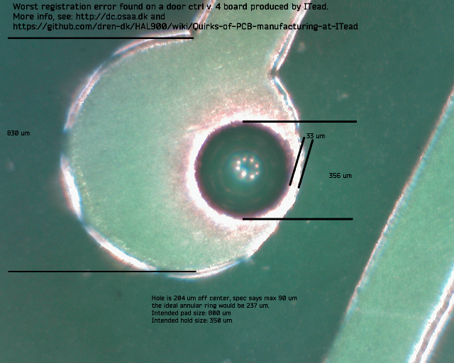 Measurements on the worst via found on any board from ITead
Laserctrl v. 1 for the PhotonSaw, a 10x10 cm PCB