Microarchitecture
This processor can be synthesized with one or more cores. Each core has a private L1 instruction and data cache, and a vector arithmetic unit. The cores share the L2 cache.

Each core has multiple hardware threads. A thread looks like an independent processor to software, with its own program counter and general purpose registers. However, threads share the arithmetic pipeline and L1 caches on their core. The purpose of multithreading is to keep these shared units busy. When a thread is waiting on a cache miss or data dependency, the core can issue instructions from other threads. A core issues an instruction from a different thread every cycle whenever possible.
When an instruction causes a data cache miss, branch, or exception, the core invalidates instructions in the pipeline that the thread issued after it. A branch resets the program counter to its destination and continues from there. A cache miss suspends the thread until the memory subsystem fills it, then resumes from the instruction that caused it.
There are 16 parallel arithmetic pipelines: one for each vector lane. Instructions with a scalar result use the lowest lane. An instruction can mix scalar and vector operands, duplicating scalar operands across all lanes. An instruction can also specify which vector lanes it updates with a mask register.
This processor uses a deep pipeline to improve clock speed. This diagram shows the execution pipeline for a single core (click to expand):
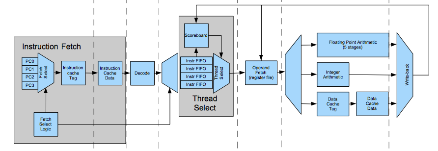
The subsequent sections describe each pipeline stage in detail.
This stage has a program counter for each hardware thread. It selects one to fetch each cycle, skipping threads that are waiting on instruction cache misses or who's instruction FIFOs (in the thread select stage, described later) are full. It increments the program counter of the issued thread, effectively always predicting branches are not taken.
The instruction cache is set associative. The default configuration has four ways. Each way has a bank of memory containing tag values and valid bits for the cache sets. This stage reads the way memories in parallel, indexing by the set id (the virtual address divided by the cache line size modulo the number of sets). Tag memory has one cycle of latency, so the next stage checks the result. Tag memory has independent read and write ports so it can process an instruction fetch the same cycle the memory subsystem fills a cache miss.
For each cache set, this stage maintains a list that tracks which ways were least recently used (LRU). A signal from the next stage updates these when there is a cache hit. This stage uses these to determine which cache line to replace when cache miss is filled.
This stage contains a translation lookaside buffer (TLB), which is a cache of virtual to physical address mappings. It looks up the address translation and passes it to the next stage. The TLB is managed by software. If a virtual address is not in the TLB, the processor raises an exception. The software exception handler routine looks up the physical address and uses special instructions to put a new mapping in the TLB. If address translation is disabled (by clearing the bit in the control register), the virtual address is treated as the translated physical address, bypassing the TLB.
When this stage detects an exception, which can be a TLB miss described in the last paragraph or other condition like a misaligned PC, it sets an exception flag that travels down the pipeline with the instruction. The writeback stage detects the exception bit is set and handles the rollback (described more in that section).
This stage compares the way tags read in the last stage to the physical address translated by the TLB (the cache is virtually indexed/physically tagged). If they match, it is a cache hit. In this case, this stage issues the instruction cache data address--formed from the way and the set indices--to instruction cache data memory. If a miss occurs, it enqueues a fill request in the instruction cache load miss queue. The L1 instruction and data caches can process requests while misses are pending, so the pipeline never stalls.
The decode stage determines which register operands the instruction needs. It extracts register indices from the instruction and maps them to register file ports. It determines which execution pipeline the instruction will be issued to, which the next stage uses to track register writeback conflicts.
The thread select stage picks an instruction from one of the threads to issue each cycle. It skips threads that it cannot issue because of operand dependencies, structural hazards, or cache misses. It uses a round robin selection policy, issuing from a different thread every cycle whenever possible. There is a FIFO of decoded instructions for each thread.
Each thread has a scoreboard, which tracks operand dependencies between instructions. There are two situations where a dependency can occur. A read-after-write dependency occurs when an instruction operand is the result of a previous instruction. In the following example, the second instruction reads register s0, which the first instruction wrote. It takes several cycles to compute the result. If thread select stage were to issue the dependent instruction too soon, it would get the stale value in the register:
    add_f s0, s1, s2
    add_f s3, s0, s4
The other type of dependency is a write-after-write dependency. If a instruction with short latency like integer arithmetic is issued after an instruction with long latency like floating point arithmetic, the second instruction can be retired before the first. If these use the same destination register, it will contain the wrong value.
A scoreboard contains a pending bit for each register, which it uses as follows:
- When the thread select stage issues an instruction, it sets the pending bit for the destination register.
- When the writeback stage updates the register file with the result of an instruction, it clears the pending bit for the destination register.
- When instructions are squashed in the pipeline by a rollback, it clears the pending bits for them.
- Before issuing an instruction, the thread select stage checks the pending bit for the source and destination registers of the instruction. If they are set, it doesn't issue the thread that cycle. Checking the source registers protects against read-after-write dependencies, and checking the destination protects against write-after-write dependencies.
Because the integer, memory, and floating point execution pipelines have different lengths, instructions issued in different cycles could arrive at the writeback stage in the same cycle. But the writeback stage can only retire one instruction each cycle. The thread select stage avoids collisions by delaying the issue of conflicting instructions (Although this sounds similar to the write-after-write logic above, that logic cannot detect conflicts between instructions issued by different threads, or instructions in the same thread that use different registers). A shift register, shared between all threads, tracks which stages have active instructions. Each thread checks the appropriate shift register bit based on latency of the next instruction it will issue.
The thread select stage tracks threads that are waiting because their store queues are full or are waiting on a data cache miss. It doesn't issue instructions from waiting threads until the data cache marks them runnable again.
The scatter/gather vector memory operations perform a separate cache access for each lane. The thread select issues these instructions 16 times with an incrementing subcycle counter signal. When a rollback occurs, the thread select stage resets the subcycle to the one that triggered it. This generic subcycle mechanism could support having fewer execution units than vector lanes or other complex instructions.
The operand fetch stage contain vector and scalar registers for all threads. The register memories have one cycle of latency. Each register file has two read ports and one write port. The writeback stage controls the write port.
This five stage pipeline performs floating point operations and integer multiplication.
| Stage | Addition | Multiplication |
|---|---|---|
| 1 | Compare exponents (and significands if exponents are equal). Use multiplexers to sort smaller and larger numbers into appropriate outputs. | Subtract exponents |
| 2 | Align smaller significand by shifting right. This stage collects guard, round, and sticky bits from the shifted out bits for rounding. | Multiply |
| 3 | Add/subtract (invert the significand for logical subtraction). Pre-normalization rounding occurs here based on GRS bits from above. | Multiply |
| 4 | Leading zero detection on significand for normalization. | Multiply |
| 5 | Normalize shift left. Post normalization rounding (only necessary for overflows). | Normalize/Round |
For addition/subtraction, stage 3 adds the significands and performs rounding simultaneously by using the rounding result to determine the carry-in bit for the adder. This is described in more detail the following papers:
- Beaumont-Smith, Andrew, et al. "Reduced latency IEEE floating-point standard adder architectures." Computer Arithmetic, 1999. Proceedings. 14th IEEE Symposium on. IEEE, 1999.
- PARK, Woo-Chan, et al. "Floating point adder/subtractor performing ieee rounding and addition/subtraction in parallel." IEICE transactions on information and systems 79.4 (1996): 297-305.
The current implementation performs multiplications in a single stage (stage 2), and passes the result through stages 3 & 4. This could use something more sophisticated like a Booth encoder/Wallace tree to reduce delay and improve clock speed (This is not critical path on FPGA, but is for ASIC synthesis). See issue #73
A single stage executes simple integer instructions like integer addition and bitwise logical operations. Despite its name, it also performs some simple floating point operations like reciprocal estimate. This stage also checks for branches.
The data cache is similar to the instruction cache. Like the instruction cache, it contains multiple tag memory banks, a least recently used list, and translation lookaside buffer. Tag memory in this stage has an extra read port to allow cache snoop operations to occur without interfering with load instructions in the execution pipeline. The cache coherence section below describes this in more detail. The translation lookaside buffer, in addition to translating read addresses, also translates store and cache control addresses that are sent to the L2 cache in the next stage.
If the request from the last stage is a cache hit, this stage reads the data from cache SRAM. It has a 512 bit wide read interface, so a contiguous vector load occurs in one cycle.
The data cache is write through. A store instruction does not directly update the L1 cache but instead inserts a request into a store queue using the physical address translated by the TLB. This then sends the request to the L2 cache, which updates the L1 cache line when it responds. Each entry in the store queue contains a full cache line. This stage aligns smaller writes to their location in the line and sets a 64 bit write mask with a single bit for each 8 bit lane. If a store occurs to an address pending in the store queue for the same thread, and it has not sent it to the L2 cache yet, the store queue updates the existing cache line with new store data (write combining). The L1 cache does not load a cache line if a store occurs to a non-resident address (it does not allocate-on-write).
When a load hit occurs, this stage checks the store queue to see if any stores are pending to that address from the same thread. If so, it forwards the store data to the writeback stage so the thread will see the new data. This avoids rolling back the thread when a write is pending.
When a load miss occurs, the L1 load miss queue searches all load miss queue entries in parallel by tag/line. If a request for that address is pending, it sets the bit in that entry's wait bitmap that corresponds to the thread. This combines the loads into one request. If the load is not pending, it allocates a new load miss queue entry.
When a load miss occurs or a thread attempts to store when the store queue is full, it rolls back the thread and suspends it. When the L2 cache responds, the load miss queue or store buffer asserts a signal to the thread select stage to wake the thread.
Non-cached device registers are in the highest range of the physical address space. Accesses to this region cause transactions on a separate request/response bus. These may only be 32-bit transfers.
This stage generates signals to update the register file. For vector register updates, it sets a mask signal with one bit for each lane to indicates which lanes to update. It extracts and aligns cache line data for memory loads and combines pending store buffer data retrieved from preceding stage.
This stage asserts the rollback control signals, which may be caused by branches or traps. These may be detected by preceding pipeline stages, which propagate it down the pipeline. Traps are precise in this architecture. The processor guarantees it will update the register file for all instructions before the instruction that caused the exception and none after. Although the processor issues instructions in-order, it may retire them out of order because the execution pipelines have different lengths. There a few reasons exceptions are handled only by this stage:
- It ensures instructions issued before the one that trapped are retired.
- It means only one rollback will be active during a cycle, since this stage only dispatches one instruction per cycle.
- If an trap occurs for a speculatively issued instruction that is subsequently rolled back (for example, instruction after a conditional branch), it will never reach this stage.
A consequence of this design is that only the memory and integer pipelines raise traps. The floating point pipeline cannot raise a precise trap because it is longer than the other pipelines by several stages. It is possible for a later instruction to retire before the trapping instruction arrived at the writeback stage. This is not a problem between the memory and integer pipeline, because the former is only one stage longer than the latter and thus instructions between them can't be retired out-of-order.
Asynchronous interrupts are handled similarly by setting a flag in the instruction fetch stage and dispatching them at the writeback stage. Although it might seem like the instruction fetch stage could simply change the PC directly, this design avoids the following scenario:
- Processor issues branch instruction
- Interrupt occurs, changes PC to new code path
- Branch instruction arrives at writeback stage and resets PC to target of branch on old code path.
If a trap occurs while a thread is waiting on a data cache miss, it resets the thread's program counter, but the thread remains suspended until the previous wait completes. This avoids race conditions that could occur when it later signals the wakeup.
Cores communicate with the L2 cache using separate request and response interfaces. When the core has a request (such as a store or load miss) to send to the L2 cache, it asserts signals on its L2 request interface. The L2 cache asserts an acknowledgment signal when it has received the request (although at that point, it has not finished processing it). Each requestor has a separate acknowledgment signal to allow arbitration between simultaneous requests. Store requests contain an entire 512 bit cache line and a 64 bit mask.
When the L2 cache finishes processing a request, it broadcasts a response on the L2 response interface, which all cores monitor. The L2 cache may respond to requests out of order because the restart mechanism (described in the next section) can reorder transactions. Identifiers in the response indicate which request it is for.
Requests to and responses from the L2 cache use physical addresses (the L2 is physically indexed/physically tagged). Address translation is performed in the processor pipeline.
The L2 cache has a four stage pipeline.
- Arbitrate Picks one request from the cores or a restarted request to forward to the next stage. The latter takes priority to avoid a deadlock if the miss queue fills up. The L2 pipeline doesn't stall, but it can stop accepting new requests from cores.
- Tag Issues memory address to tag memory which has one cycle of latency. It also reads dirty bits.
- Read If this is an L2 cache hit, read the cache data, which it will send in the L2 response. If this transaction is a fill, reads the dirty evicted line, which it will put in the writeback queue. Asserts signals to update tag memory if needed.
- Update Issues signals to update cache memory, combining with previously read data for each byte where the store mask is set.
The L2 cache is write-back and allocates cache lines both on load and store misses. When a cache miss occurs, the L2 cache places the request in a miss queue. A state machine controls loading data from external memory. When the transaction finishes, the request restarts at the beginning of the L2 cache pipeline with the fetched data.
A writeback queue holds data that it will store back to main memory. The L2 cache processes requests in the writeback queue before those in the load miss queue to avoid loading stale data.
The L2 cache uses the AMBA AXI protocol to communicate with main memory. One module encapsulates protocol handling. An alternate module could be substituted to support different bus protocols (for example, Wishbone).
The L2 cache is not inclusive or exclusive: A cache line may only be in the L1 cache, only in the L2 cache, or in both.
To simplify software, this processor supports a coherent address space, shared across all threads and cores. A coherent cache obeys three rules:
- If a thread writes to a memory location and later reads back from it, with no other thread writes to the location between, it must get the same value back.
- When a thread writes to a location other threads must eventually see it.
- All other threads must see stores in the same order (although not necessarily the order the stores occurred).
The L1 data cache uses a snooping write-update protocol. Because the cache is write-through, there are no 'dirty' or 'exclusive' L1 cache lines as there would be in a write-back cache, so it doesn't need a complex protocol to get exclusive access to a line. But it does need to update L1 data cache lines in other L1 caches whenever a write occurs.
Bypass logic in the store queue enforces rule 1 by making a pending store visible to the thread that issued it. The write update mechanism enforces rule 2. All writes go first to the L2 cache without updating the L1D cache, which serializes the results. This enforces rule 3. The store bypass logic does not make writes visible to other threads on the same core for the same reason.
Each core snoops L2 responses for store updates. A three stage pipeline in each core processes messages from the L2 cache. This logic handles store updates and L1 load miss fills:
- The first stage sends the address from the response to L1D tag memory to determine if it cached. L1D tag memory has a dedicated read port for snoops so this can occur in the same cycle as a load from the instruction pipeline.
- The second stage checks the result from tag RAM a cycle later. If the data is not already cached, the pipeline asserts signals to update tag RAM.
- The third stage updates data memory a cycle after tag memory. This must be done here rather than in the second stage to avoid a race condition, because the execution pipeline reads data memory a cycle after checking the tag.
The snoop address from the L2 cache is a physical address, but the L1 tags are indexed by virtual address. It is not necessary to translate the address if the number of sets (which is a configurable synthesis option) is 64 or fewer. In this case, the set index is the same for virtual and physical addresses, because the set index wraps on a page boundary (4k) or smaller. Additionally, if the number of sets were greater than 64, there would be a problem with cache aliasing, because the same physical address mapped at two virtual addresses (a cache synonym). So, to simplify the hardware, the number of sets is restricted to 64 on a MMU enabled configuration. With four sets, this allows a 16k L1 cache. For a larger cache, higher associativity can be configured: a 8-way set associative data cache will be 32k.
This processor uses a relaxed memory consistency model. Because the pipeline issues memory instructions in order, it preserves read-to-read, and write-to-write ordering. But it cannot guarantee write-to-read ordering between threads because execution of a thread can proceed while a write is in the store queue. The membar (memory barrier) instruction enforces explicit ordering by suspending the thread if a pending store is in in the store queue. When the L2 cache acknowledges it, it resumes the thread. This guarantees all other L1 caches have the stored data.
If a store writes a full line to the L2 cache as a block vector store and the line is not cache resident, it doesn't load it from memory--which would be unnecessary--but instead puts the new data into the line.
Synchronized loads/stores are similar to load linked/store conditional instructions on other processors. They enable atomic read-modify-write operations and allow creating primitives like spinlocks, atomic variables, and lock-free/wait-free data structures.
A synchronized store should follow a synchronized load. When a thread executes a synchronized memory load, the L2 cache latches the address of the load (it tracks each thread independently). If another thread writes to that cache line, it clears this address. Synchronized store operations check the latched address. If it doesn't match, the synchronized store fails and it copies zero into the source register of the instruction. If it does match, the store proceeds and it copies one into the source register.
To operate correctly, a synchronized load must atomically set the internal register in the L2 and return the current data in the line. Synchronized loads behave like L1 cache misses to ensure this. The cache load miss queue handles this request.