The aim of this project is to create an easy way, HDL implemented, to visualise data coming from the analog to digital converter (ADC) mounted onto the FPGA developement board. In this way, it is possible to characterise the ADC, perform some tests on the ADC performances, test some Digital Signal Processing (DSP) modules or to sample analog signals.
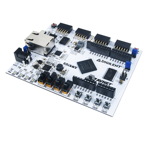
- The FPGA developement board used is the ARTY A7 by Digilent on which there is tha Artix-7 35T FPGA by Xilinx
- The software used is Vivado 2021.1 by Xilinx
- The HDL language used is SystemVerilog
-
Using the IP integrator (IP catalogue) in Vivado, it has been possible to instantiate the XADC module into the design. The Artix-7 FPGA has inside the XADC chip which is the analog to digital converter provided by Xilinx.
-
A particular Wrapping circuit has been built in order to create a simple interface accessible from other eventual modules.
-
A module called "Printer_UART" has been developed in order to print on screen the data sampled by the XADC.
-
The system has also inside a chronometer to store the time at which the sample has been recorded.
-
A "Pulse generator" is aimed to the generation of the signal triggering the sampling process. Here, by sampling process, I mean that the pulse will enable the printer to send the data via the UART cable to a computer.
-
To read the data from the UART cable it is possible to use a terminal like "PuTTY".
-
In this specific implementation, the sampling frequency (in this case I am referring to the samples displayed on the PC screen and not the actual sampling frequency of the XADC) is 1 Hz. However, this frequency can be changed in the top module changing the period of the PULSE_GENERATOR.
In the picture below you can see the data sent by the FPGA via the UART cable.

The numbers displayed represents the following data:
- First column: Time expressed in milliseconds. Since the sampling frequency set up is 10Hz you can see that the least significant digits are zero.
- Second column: The digitalised output from the pin A0.
- Third column: The digitalised output from the pin A1.
- Fourth and Fifth column: Eventual digitalised output from pin A2 and A3. In this case the XADC is configured only for the acquisition of the channels A0 and A1. Therefore the two last columns are populated by the constant value 2048 (see later for the reason why it is 2048 and not 0).
- The XADC has been configured in the "Bipolar mode". This means that it can digitalise voltage signals in the range -1.5 V to +1.5 V. The resultant digitalised number is returned in the bipolar binary notation. This means that a negative signal is coded with the 2's complement.
- Since in the output I didn't want to print the + and - characters, I translated the numbers from the bipolar notation to the unipolar notation. Then, I had to negate the most significant bit. To understand better see the following example:
EXAMPLE no.1 :
- Input = 0 V
- Digitalised input = 000000000000
- From bipolar notation (000000000000) to bipolar notation 1000000000000
- From binary to decimal we obtain 2^(12-1) = 2^11 = 2048
EXAMPLE no.2:
| Bipolar | Bipolar decimal | Unipolar | Unipolar decimal |
|---|---|---|---|
| 011 | 3 | 111 | 7 |
| 010 | 2 | 110 | 6 |
| 001 | 1 | 101 | 5 |
| 000 | 0 | 100 | 4 |
| 111 | -1 | 011 | 3 |
| 110 | -2 | 010 | 2 |
| 101 | -3 | 001 | 1 |
| 100 | -4 | 000 | 0 |
To build up the design I have used some IPs by Xilinx. These modules can be configurated from the IP catalogue in Vivado. To create your personal module follow these steps:
- Click on IP catalogue in the Project flow navigator
- Search for the desired IP. In our case the IPs used are the XADC Wiziard and the FIFO generator
- Click on the IP desired
- Customize the IP according to the fatures required
- Click on Generate IP instance
- Then you have to generate and synthesise the required files (Click on Generate in the pop-up window).
- In the file manager, where you can see the Source Hierarchy click on the IP sources panel.
- In the path: IP_COMPONENT_NAME >> Instantiation template >> ... youìll find the two Instantiation templates, one written in Verilog HDL and the other in VHDL. Now you can instantiate your customised module into your design.
If you change the number of channels in the top module, then you need to open the "XADC Wiziard" in Vivado software, change the "Sequenced channels" and re-run the synthesis of the component XADC. When the synthesis is finished you need to open the file "NAME_stub.v" in the IP resources, copy the code
      .INIT_40(16'h0000),
      .INIT_41(16'h21A0),
      .INIT_42(16'h0400),
      ...
and replace the part contained in the file "NAME_netlist.v". This is required because the XADC module comes from an IP by Xilinx and to set up properly the sequencer settings you need to generate the encrypted sources. In principle one could change by hand the registers in the instantiation (.INIT_40(1b'h...)). This procedure, however, is quite tedious since it is required to know the meaning of all these registers. The procedure exploiting the XADC wiziard is more "user friendly" even if it is a bit longer. After generating the correct template for the XADC module you need to "disable the source file" using the Vivado navigation menu. This because in the xadc_netlist.v file there are the instructions used by vivado to generate the required sources and so the IP generated via the IP catalogue is unnecessary.
Here some useful online resources which I have used to develope this simple ADC sampler:
- Digilent reference webpage (Arty A7) : https://digilent.com/reference/programmable-logic/arty-a7/start
- Arty A7 reference manual : https://digilent.com/reference/programmable-logic/arty-a7/reference-manual
- OpenCores (a useful web platform where it is possible to find HDL open source cores) : https://opencores.org/
- Companion website for the book FPGA prototyping by SystemVerilog examples by Dr. Chu : https://academic.csuohio.edu/chu_p/index.html
- Xilinx Vivado website: https://www.xilinx.com/products/design-tools/vivado.html
- Digilent GitHub repositories : https://github.com/digilent
To build up a Vivado project, the following operations are required:
- Open Vivado
- Click on New project
- Give a name to the project and click on Create project subdirectory and click on Next
- Click on RTL project. Then, click Next
- Now choose all the sources files .v (if the files are written in verilog), .sv (if they are written in SystemVerilog), .vhd (if files are written in VHDL), click on Scan and add RTL include files into the project and Copy sources into project. Then, click on Next
- Import the Costraint file .xdc in the same manner as before.
- Now you need to select the Target device. To do this, select the Boards menu and search for ARTY A7-35T. To do this operation you need to install on your computer the Digilent boards files. This procedure is described at the following link https://digilent.com/reference/programmable-logic/guides/installing-vivado-and-vitis if you use the latest versions of Vivado and Vitis unified platform or the following link https://digilent.com/reference/programmable-logic/guides/installing-vivado-and-sdk if you use Vivado and Vivado SDK.
- Now it is possible to modify the project, run the synthesis, the implementation and the bitstream generation