Home
Warren Stearn's original wire-wrap prototype FlipChip tester was interfaced to a PC parallel port. The C code that Warren wrote used porttalk to get to the parallel port and bit-bashed 5x SPI buses running at 140 kHz connected to the SPI GPIO chips on the tester. This worked fine as long as you like to work with a CLI, had a real parallel port on your PC, and were not running an OS newer than Windows 7.

Warren passed away in 2017 and in 2018 his FlipChip tester software and design were put in the public domain. Vince Slyngstad made an Eagle PCB design of the original FlipChip tester that still uses the PC parallel port interface and Warren's original software.
Since PCs with parallel ports are scarce we modified Vince's PCB by cutting and jumpering traces to bus all of the SPI GPIO chips together, and to configure each SPI GPIO chip with a unique hardware address.
Two USB/SPI cables are available from FTDI. It shouldn't make a different which one you use. C232HM-DDHSL-0 supplies 3.3V, This is the one that I bought. C232HM-EDHSL-0 supplies 5.0V The SPI cable works up to 10MHz with the MCP23S17 GOIP part.
Cable Wiring Color Pin Number Name Type Description MCP23S17 Pin Red 1 Vcc Output 3.3V @ 250mA source 9 Orange 2 SCK SK Output Serial Clock 12 Yellow 3 MOSI DO Output Serial data output 13 Green 4 MISO DI Input Serial Data Input 14 Brown 5 #CS CS Output Serial Chip Select 11 Gray 6 GPIOL0 Input/Output General Purpose input/output Purple 7 GPIOL1 Input/Output General Purpose input/output White 8 GPIOL2 Input/Output General Purpose input/output Blue 9 GPIOL3 Input/Output General Purpose input/output Black 10 Gnd Gnd Device ground 10
#CS ADBUS3 GPIOL0 ADBUS4 GPIOL1 ADBUS5 GPIOL2 ADBUS6 GPIOL3 ADBUS7 RedLed ACBUS6 GrnLed ACBUS8 XtrnPwr ACBUS9
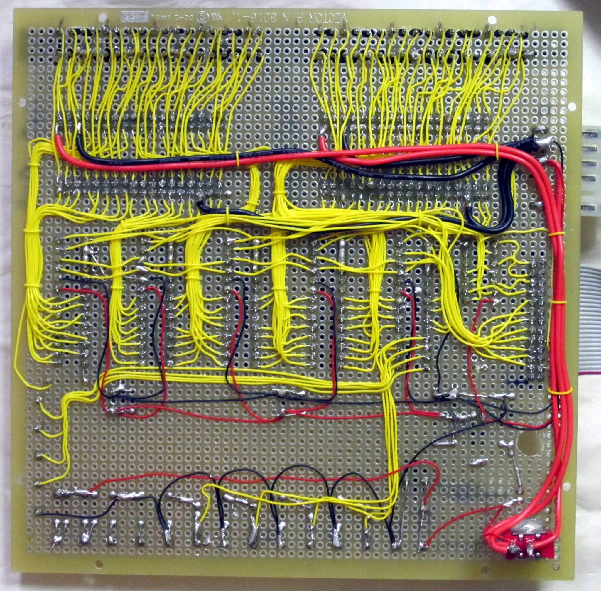
Modifications to the original FlipChip Tester PCB for the USB/SPI interface:
Add 10k pullup from IC5-18 (RESET-N) to Vdd.
Cut A0(15), A1(16), A2(17) to RESET-N(18) traces for all 5x SPI chips.
Jumper all 5x RESET-N(18) pins together.
IC5-18 is already connected to PC1-4.

These modifications set the SPI Hardware Addresses of each IC to match the IC number.
	Add 10k pullup from IC1-15 to Vdd.
	Add Ground to IC1-16, 17.
	Add 10k pullup from IC2-16 to Vdd.
	Add Ground to IC2-15, 17.
	Add 10k pullup from IC3-15, 16 to Vdd.
	Add Ground to IC3-17.
	Add 10k pullup from IC4-17 to Vdd.
	Add Ground to IC4-15, 16.
	Add 10k pullup from IC5-15, 17 to Vdd.
	Add Ground to IC5-16.

Do not install IC6. This IC location can be used to jumper the SO and SI signals together.

Connect SO at IC6-1, 3, 4, 5, 9, 11 together.
	SO will be on PC1-26

Connect PC1-10, 12, 14, 16, 18 together.
	SI will be on all of these pins.

USB SPI connections on connector PC1:
	Color	Pin Number	Name	Type		Description			Connector PC1
	Red	1		Vcc	Output		3.3V @ 250mA source		4 for the RESET-N pullup
	Orange	2	SCK	SK	Output		Serial Clock			8
	Yellow	3	MOSI	DO	Output		Serial Data output		10
	Green	4	MISO	DI	Input		Serial Data Input		26
	Brown	5	#CS	CS	Output		Serial Chip Select		6
	Gray	6		GPIOL0	Input/Output	General Purpose input/output
	Purple	7		GPIOL1	Input/Output	General Purpose input/output
	White	8		GPIOL2	Input/Output	General Purpose input/output
	Blue	9		GPIOL3	Input/Output	General Purpose input/output
	Black	10		Gnd	Gnd		Device ground			25

	In the future I will connect one of the unused CS lines to the RESET-N signal.
	The tester seems to work OK without it.
The USB/SPI cable to interface the PC to the FlipChip tester is an FTDI C232HM-DDHSL-0. Digi-Key, Farnell, and Mouser usually have lots of them in stock for about $40. You can find technical details on the USB/SPI cable here: http://www.ftdichip.com/Products/Cables/USBMPSSE.htm
You must replace the standard Windows driver for the USB/SPI cable with the FTDI D2XX driver. You can download the Windows D2XX driver and installation guide here: http://www.ftdichip.com/Drivers/D2XX.htm
The FTDI LibMPSSE-SPI library provides the SPI protocol for this application. A wrapper library, FTD2XX_NET.dll, provides an interface between this managed code application and the unmanaged code LibMPSSE-SPI library. Both the libMPSSE.dll and libMPSSEWrapper.dll files need to be in the same directory as the Warrens_Flipchip_Tester.exe file.
The FlipChip Tester needs to be supplied with +5V to power the FlipChip and the SPI GPIO chips.
The toggle switch needs to be set towards the right to enable +5V power to the FlipChip. The amber LED will illuminate when the +5V power to the FlipChip is on. You should turn off the +5V when installing or removing a FlipChip.
The Green LED will turn on at the beginning of a test, and will stay on as long as no faults are found. The Yellow LED will illuminate when a test is running. The Red LED will illuminate if a fault is found during a test.
Before you can use Hardware Adressing, you need to write 0x08 to the IOCON register. There is a bug in the MCP23S17 so you need to send the Hardware Address configuration to an address of 0x00 and 0x07. The SPI command is: 0x40 0x0a 0x08 0x08 and 0x4e 0x0a 0x08 0x08
IC IOLAT Register to GP Pin Name Mapping
GPB7..GPB0 GPA7..GPA0

IC/Pin to DEC Connector Pin Mapping
IC0, GPB7, AA1 PIN 0
IC0, GPB6, AB1
IC0, GPB5, AC1
IC0, GPB4, AD1
IC0, GPB3, AE1
IC0, GPB2, AF1 PIN  5
IC0, GPB1, AH1
IC0, GPB0, AJ1
IC1, GPB7, AK1
IC1, GPB6, AL1
IC1, GPB5, AM1 PIN 10
IC1, GPB4, AN1
IC1, GPB3, AP1
IC1, GPB2, AR1
IC1, GPB1, AS1
IC1, GPB0, AT1 PIN 15 is PIN_GROUND_AT1
IC2, GPB7, AU1
IC2, GPB6, AV1
IC0, GPA7, AA2 PIN 18 is PIN_POWER_AA2
IC0, GPA6, AB2
IC0, GPA5, AC2 PIN 20 is PIN_GROUND_AC2
IC0, GPA4, AD2
IC0, GPA3, AE2
IC0, GPA2, AF2
IC0, GPA1, AH2
IC0, GPA0, AJ2 PIN 25
IC1, GPA0, AK2
IC1, GPA1, AL2
IC1, GPA2, AM2
IC1, GPA3, AN2
IC1, GPA4, AP2 PIN 30
IC1, GPA5, AR2
IC1, GPA6, AS2
IC1, GPA7, AT2
IC2, GPA0, AU2
IC2, GPA1, AV2 PIN 35
IC2, GPB5, BA1 PIN 36
IC2, GPB4, BB1
IC2, GPB3, BC1
IC2, GPB2, BD1
IC2, GPB1, BE1 PIN 40
IC2, GPB0, BF1
IC3, GPB7, BH1
IC3, GPB6, BJ1
IC3, GPB5, BK1
IC3, GPB4, BL1 PIN 45
IC3, GPB3, BM1
IC3, GPB2, BN1
IC3, GPB1, BP1
IC3, GPB0, BR1
IC4, GPB7, BS1 PIN 50
IC4, GPB6, BT1 PIN 51 is PIN_GROUND_BT1
IC4, GPB5, BU1
IC4, GPB4, BV1
IC2, GPA2, BA2 PIN 54 is PIN_POWER_BA2_NC (no connection)
IC2, GPA3, BB2 PIN 55
IC2, GPA4, BC2 PIN 56 is PIN_GROUND_BC2
IC2, GPA5, BD2
IC2, GPA6, BE2
IC2, GPA7, BF2
IC3, GPA0, BH2 PIN 60
IC3, GPA1, BJ2
IC3, GPA2, BK2
IC3, GPA3, BL2
IC3, GPA4, BM2
IC3, GPA5, BN2 PIN 65
IC3, GPA6, BP2
IC3, GPA7, BR2
IC4, GPA0, BS2
IC4, GPA1, BT2
IC4, GPA2, BU2 PIN 70
IC4, GPA3, BV2
IC4, GPA4, PROBE_1 PIN 72
IC4, GPA5, PROBE_2
IC4, GPA6, PROBE_3
IC4, GPA7, PROBE_4 PIN 75
IC4, GPB0, GREEN  LED
IC4, GPB1, RED    LED
IC4, GPB2, YELLOW LED
IC4, GPB3, RED2   LED
We noticed that the performance of the SPI bus was significantly less than expected. We wrote a C# application SpitestGui to talk to a MCP23S17 SPI GPIO parts using a C232HM-DDHSL-0 cable so we could measure the SPI performance.
During a SPI register write the SPI CS goes active (low), The SPI bus is idle for 243 us, The SPI SK, SO, and DI signals are active for 16 us, The SPI bus is idle for 243 us, The SPI SK, SO, and DI signals are active for 16 us, The SPI bus is idle for 1300 us, The SPI CS goes inactive (high).
With this timing we can only get one SPI transaction every 2.0 ms. During the 2 ms transaction the SPI bus is idle for more than 1300 us. Using this time we can only utilize 1.6% of the SPI bus bandwidth.
Rewriting the FTDi SPI library to delete the delays would dramatically improve the SPI performance and the performance of the FlipChip tester.
Copyright (C) 2018-2021, The Rhode Island Computer Museum
This program is free software: you can redistribute it and/or modify it under the terms of the GNU General Public License as published by the Free Software Foundation, either version 3 of the License, or (at your option) any later version.
This program is distributed in the hope that it will be useful, but WITHOUT ANY WARRANTY; without even the implied warranty of MERCHANTABILITY or FITNESS FOR A PARTICULAR PURPOSE. See the GNU General Public License for more details.
You should have received a copy of the GNU General Public License along with this program. If not, see https://www.gnu.org/licenses/.
Author(s): Michael Thompson mike@ricomputermuseum.org