Technical Documentation
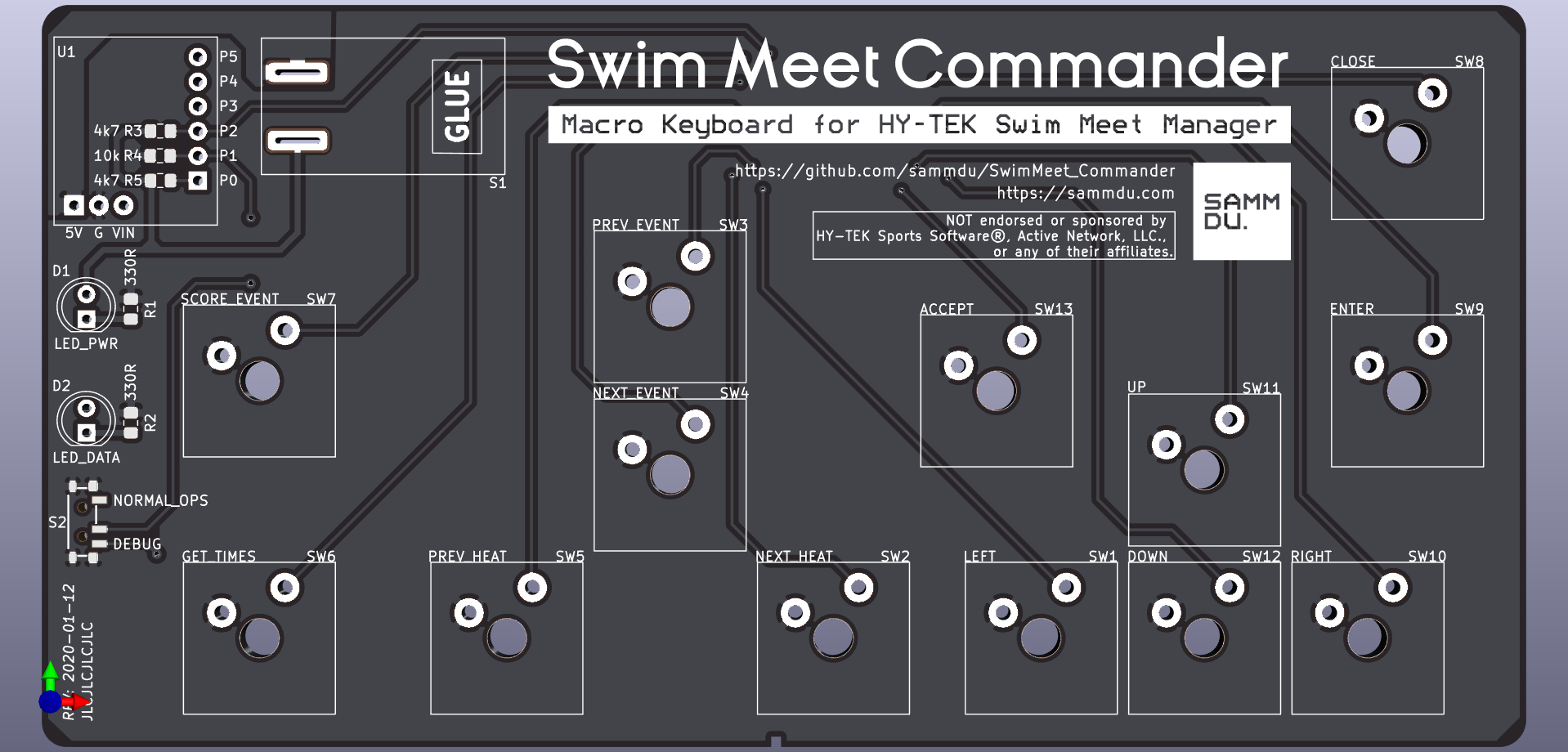
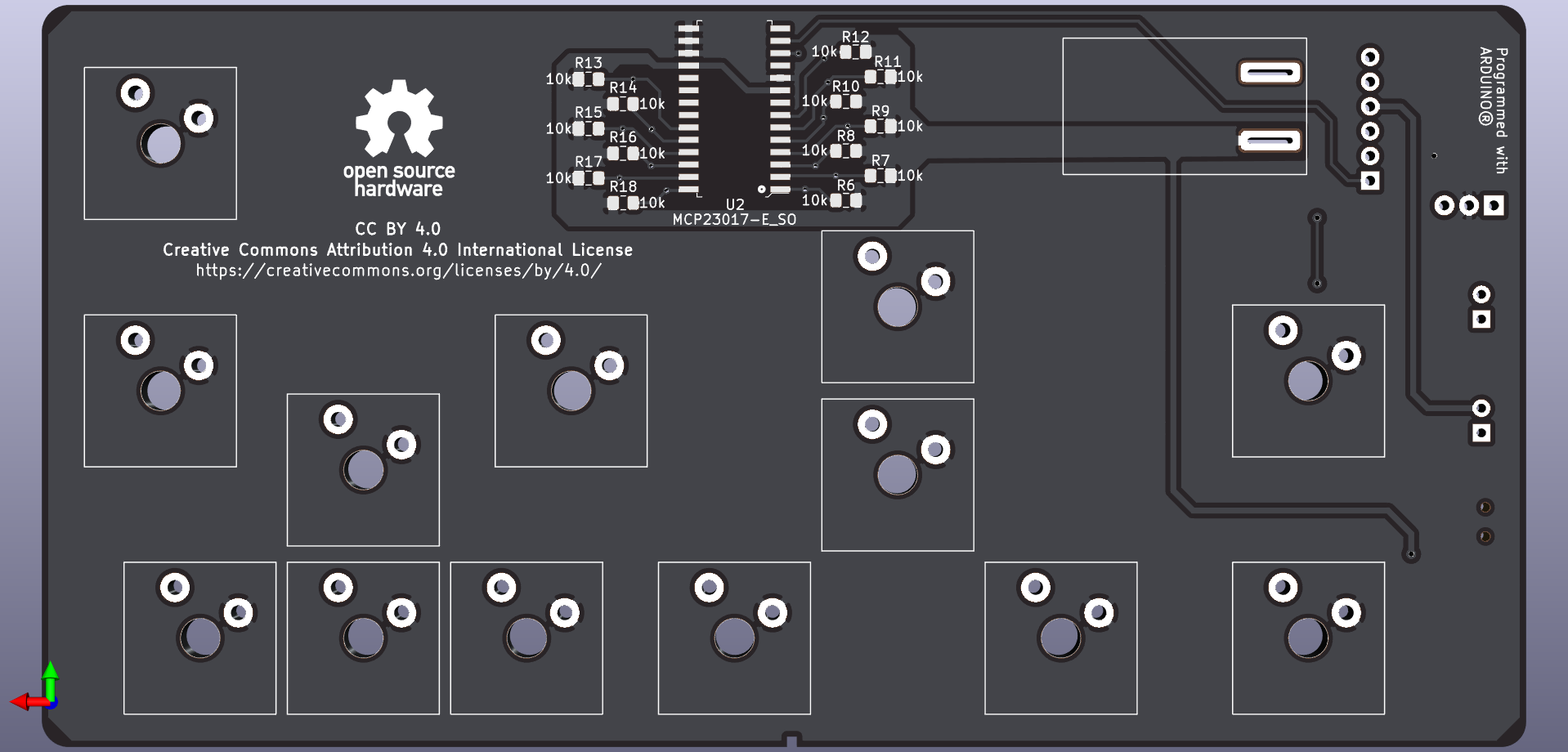
The PCB has 2 copper layers.
🔗 See Gerber Production Files (Revision: 2020-01-12)
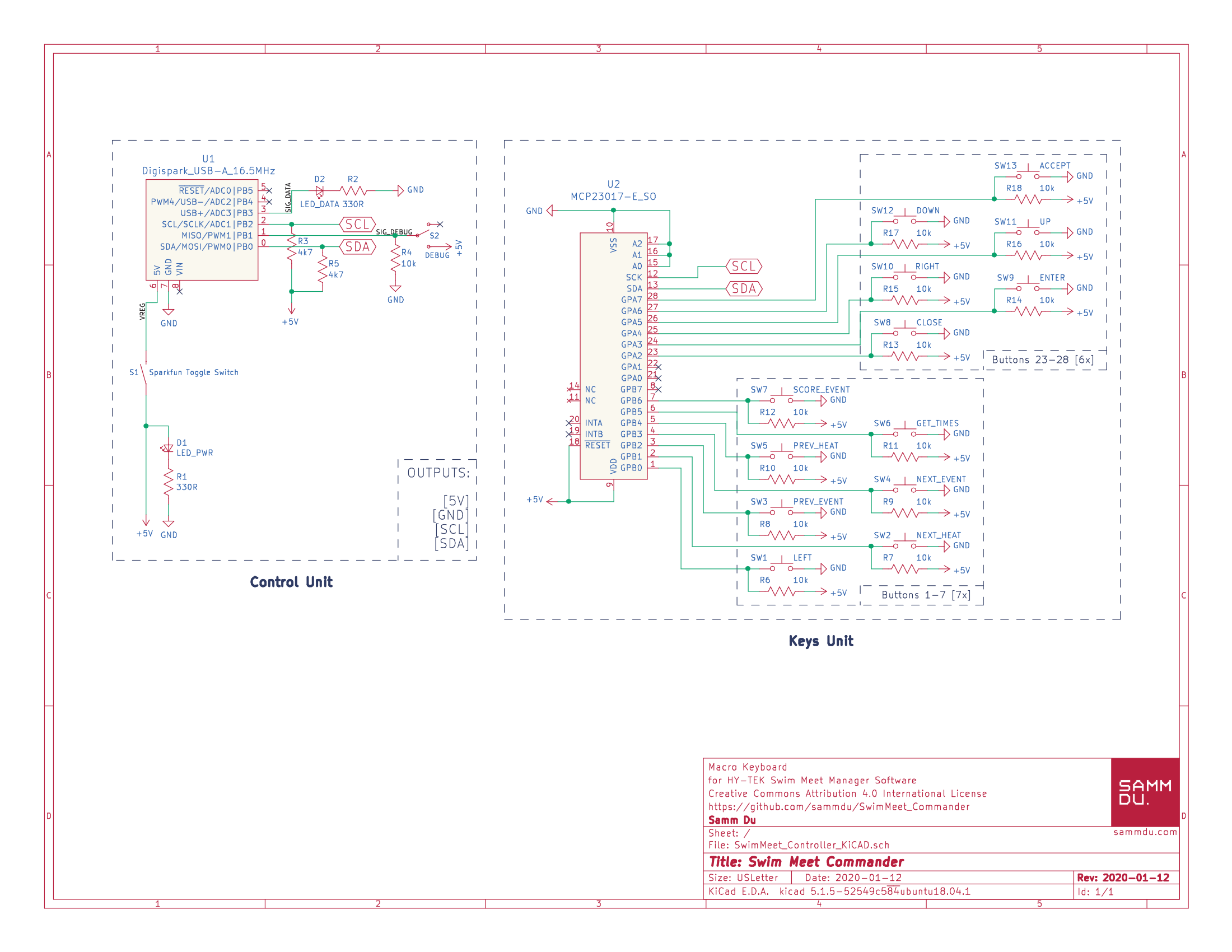
Note: For the MCP23017 IO expander, the GPIO-A memory pointer is 0x12, GPIO-B memory pointer is 0x13.
Every input pin of the MCP23017 is pulled up to 5V by a 10kOhm resistor, making them active-low.
| Functionality | Keyboard Shortcut | Physical Key | IC Pin | GPIO Group | I2C Reading |
|---|---|---|---|---|---|
| Score Event |
Ctrl+S
|
SW7 |
7 | B | 0b10111111 |
| Get Times | F3 |
SW6 |
6 | B | 0b11011111 |
| Previous Heat | F4 |
SW5 |
5 | B | 0b11101111 |
| Next Heat | F5 |
SW2 |
2 | B | 0b11111101 |
| Previous Event |
Ctrl+F4
|
SW3 |
3 | B | 0b11111011 |
| Next Event |
Ctrl+F5
|
SW4 |
4 | B | 0b11110111 |
| Up Arrow | ↑ |
SW11 |
26 | A | 0b11011111 |
| Down Arrow | ↓ |
SW12 |
27 | A | 0b10111111 |
| Left Arrow | ← |
SW1 |
1 | B | 0b11111110 |
| Right Arrow | → |
SW10 |
25 | A | 0b11101111 |
| Accept Discrepancy |
←, pause, Enter
|
SW13 |
28 | A | 0b01111111 |
| Enter | Enter |
SW9 |
24 | A | 0b11110111 |
| Close Window |
Alt+F4
|
SW8 |
23 | A | 0b11111011 |
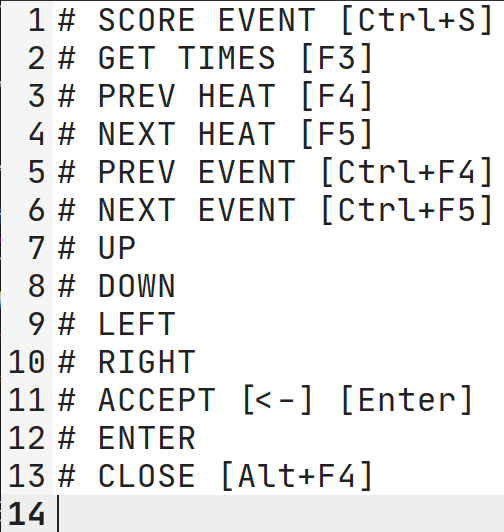
There is a debug switch built-in to the device located at the bottom-left side of the device, schematically notated as S2, shown below by the green box.
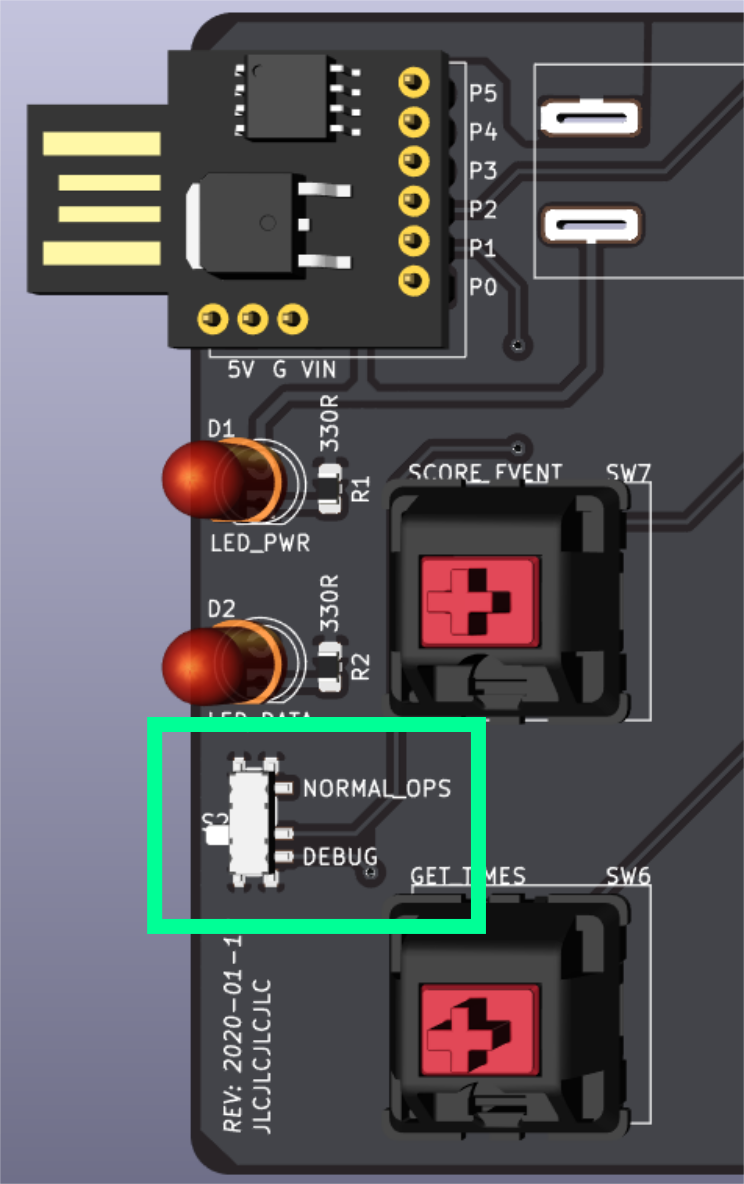
When in NORMAL_OPS (top) position, the device functions normally, sending intended keyboard shortcuts.
When in DEBUG (bottom) position, the device goes into debug mode. When a key is pressed, it will type out the intended functionality and keyboard shortcut into any text box.
Below is a sample output into a text editor of pressing every key once in debug mode.