Hermes Lite 2.0
This document describes the architecture planned for Hermes-Lite 2.0, subsequently referred to as v2. The goals for v2 are as follows:
- Continue low-cost focus of Hermes-Lite. This includes a QRPp build option of less than $100 for DIY types.
- Support a "fat pipe" to be able to better trade off computation between software and hardware. A longer term goal is to move more computation from the FPGA to software to reduce cost and complexity as well as improve maintainability.
- Eliminate cost, complexity and fragility of too many connectors.
- Provide better "hooks" for expriments and extension. This includes LVDS and SPI.
- Eliminate dependency on BeMicro as connector is costly and awkward, future is unpredictable, and has limited family member choices.
- Improve form factor to allow enclosure with extruded aluminum enclosures.
- Accomodate easy interfacing to various PAs.
- Make base unit stand alone such that it can be a QRPp transceiver or test instrument without additional circuitry.
- Evolve and reuse the v1.22 design as much as possible. Layout involving the AD9866 will be reused. Version 1.22 firmware will run on v2 with little change.
- Avoid second system effect...
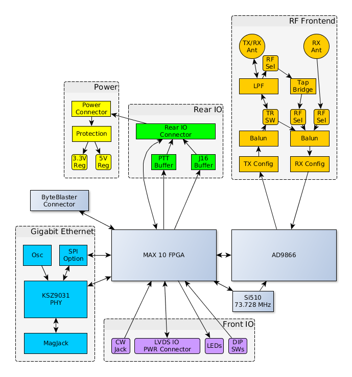
Pictured below and available here as a PDF is the v2 architecture block diagram. Subsequent sections in this document will refer to and describe the various blocks.
At the core of v2 is still the AD9866 cable modem chip. This continues with the same low cost solution at the heart of previous Hermes-Lites.
All three CFG pins will be connected to the FPGA. This will allow to run in full-duplex mode always yet achieve half-duplex savings by powering down internal blocks to emulate half-duplex. Supporting only one interface (full-duplex) simplifies what is currently done in v1.2. Besides these CFG pin changes, TX config changes described in the RF Frontend section and clocking changes described next, the use of the AD9866 will be as proven in v1.2.
- 31 pin estimated FPGA pin budget
- $27-$33 estimated cost
V2 will still use the same Silicon Devices 73.728 MHz oscillator as used in v1.2. This oscillator has exhibited good performance in terms of clock jitter and phase noise. The Si510 output enable will be connected to the FPGA. The Si510 clock will be connected to the AD9866 as in v1.2 but also to the FPGA in v2. This configuration will allow us to disable the Si510 and supply an alternate clock from the FPGA. Fanning out the clock connection from the Si510 to the AD9866 and FPGA has been tested experimentally on v1.2 without issue. During layout, the Si510 will be placed in a location to reduce effects of the AD9866 heating up and down during TX and RX.
- 2 pin estimated FPGA pin budget
- $5 estimated cost
V2 will use an onboard Altera MAX 10 FPGA instead of a BeMicro card. V2 will use the SC parts in 144-pin EQFP package. Design will be for the least expensive speed grade, typically C8. This provides the following advantages:
- The MAX 10 is based on the Cyclone IV architecture as seen in the SDK and shown to work with the Hermes-Lite.
- Devices ranging in size from 2K to 50K FPGA LE (logic elements) exist with the same footprint. This allows for future cost reduction by reducing the size of the FPGA. The cost ranges from under $10 to $57. Currently, the Hermes-Lite uses a 25K LE FPGA. This range allows for firmware with 5-7 and possibly more receivers at the 50K size down to 1 receiver and SPI interface at the 2K-4K size.
- The "S" MAX 10s support use of a single power supply of 3.3V. This reduces voltage regulation costs and simplifies board layout.
- The "C" MAX 10s have embedded flash and do not require an external configuration EEPROM. This reduces cost and simplifies layout.
- The EQFP package has all pins exposed to permit assembly by hobbyist and requires only a 4 layer board. A BGA package would require more layers. A BGA package does have a reduced footprint but PCB area costs are insignificant ($0.045 per square centimeter). Currently, the EQFP MAX 10 parts are less expensive than BGA counterparts. Also, the EQFP package is the only one common for device sizes from 2K LE to 50K LE.
- This choice eliminates dependency on BeMicro. MAX 10 devices are available from DigiKey. Several contacts at Altera and Altera distributors have said the 50K part will be available in 2015Q4.
There will be no dedicated oscillator for the MAX 10. Instead, the Si510 and/or KSZ9031 will provide clocks to the MAX 10.
- $10-$57 estimated cost
V2 will not have an onboard byteblaster programmer for the FPGA due to copyright restrictions. Instead, early adopters will have to buy a less than $10 clone from Amazon or e-bay. A byteblaster header will be included on v2.
Later iterations of v2 firmware will have the option to program over ethernet. Two images will be stored in the MAX 10 flash: rescue for programming and the current SDR image. The rescue image will be difficult if not impossible to overwrite so that the user can always rely on ethernet programming of the flash.
Some rough cost analysis of a BeMicro CV with 25K LE and SamTec connector shows that cost is pretty much equivalent to a MAX 10 25K LE device plus ByteBlaster clone. The cost savings comes when the size of the FPGA is reduced. The MAX 10 alternative also provides 50K LE at only about $10 more, option for gigabit which is not available on the CV, and reduction in complexity by eliminating the SamTec connector.
- $0-$10 estimated cost
The V2 power connection consist of power connector, protection, 3.3V regulation and optional 5V regulation.
This will be a simple screwdriver-friendly two connection terminal block as discussed in this thread. The power connector is intended to be used when no PA board is plugged into the rear IO. When a PA board is plugged in, the PA will supply 7 to 36 volts via the rear IO connector. Since a PA board demands significant and unpredictable current, v2 will not provide the power supply for a PA.
- <$1 estimated cost
Since the power connector is unkeyed, protection will be provided by a FET device as discussed in this thread.
- <$1 estimated cost
Voltage regulation will be done in similar fashion to what is described in this thread. The part is available from DigiKey. This power supply was used in these tests without impact on noise.
The discrete components used in this power supply will be used on the v2 PCB rather than the current miniature PCB. This allows for a wider selection of devices, setting of the switching frequency and better control over the critical inductor. With the largest FPGA, the Hermes-Lite (AD9866, FPGA, Ethernet, IO) will need at least a 2.5A power supply. The switching regulators have been narrowed down to:
- MP2467 as used in original power supply
- MP1584 with 1.5 MHz adjustable switching frequency
- MP2560 with 4 MHz adjustable switching frequency
These (and other device not listed) share the same footprint and support circuitry. We can use the MP2467 as the most conservative choice which matches what has been proven already. The other two device offer different and adjustable switching frequencies. Although noise expected from switching should be low, we can pick a frequency such that it and all harmonics fall outside of amateur radio bands.
Inductor choice is important in minimizing switching noise. See this and this.
Support for input voltages ranging from 7V to 28V should allow for some interesting external power supply options and PAs with higher output.
- $2-$4 estimated cost
As described and tested in this thread, 5V is no longer required and will be eliminated.
V2 will provide onboard relay drivers for J16-style relay switching, PTT buffer, as well as a few additional IO signals on the rear IO connector. These additional IO will be for slow signal switching and come directly from the FPGA. They are intended only for v2-specific companion PAs.
- 4 pin estimated FPGA pin budget for additional IO
The rear IO connector will be a common right angle DIL 0.1 inch type, either header or receptacle. This selection is for easy interfacing to custom companion PA boards, or easy wiring to an external PA.
- $1 estimated cost
Similar to the Hermes, a ULN2003LVPWR type relay driver for 7 signals will be used. A device with family members that support 5V or 12V relays at build time will be used.
- 7 pin estimated FPGA pin budget
- <$1 estimated cost
This will be similar to the Hermes and provide external PTT output for a PA.
- 1 pin estimated FPGA pin budget
- <$1 estimated cost
To support interesting new SDR applications requiring a fat pipe, v2 will include gigabit ethernet. The basic ideas and RTL have been proven on a BeMicro CVA9 with a v1.22. The extra cost for gigabit over dp83848-based megabit ethernet is $5-$6.
Draft schematic and BOM can be found on Google Drive.
The gigabit ethernet block is a straight-forward implementation following the datasheet recommendations as well as the Hermes and BeMicro CVA9 designs. Noteworthy differences and design decisions are described below.
- The Hermes and BeMicro CVA9 use the KSZ9021. V2 will use the KSZ9031. This is essentially a newer version of the part with lower current requirements. It is also available with less expensive copper bonding.
- The Hermes uses a 64 pin version, the BeMicro CVA9 a 48 pin version. V2 will use a 48 pin version to save space.
- This PHY chip requires a low current 1.2V supply. It includes an LDO controller for an external FET to save costs. After investigating costs in dollars and area, I chose to go with a small switching regulator as it had comparable costs but did not waste 650 mW of power. The Hermes uses an LDO, the BeMicro CVA9 a different switching regulator. Micrel publishes app notes describing 3 variations to provide power, and small switching regulator is one option.
- The PHY chip requires a 25 MHz clock. In standard builds, this will be supplied by the VersaClock generator to save the cost of the oscillator. There is also the option to connect a local oscillator. This oscillator was picked for its small size, relatively low cost and acceptable specs.
- The PHY chip can provide the MAC (FPGA in V2) with a 125 MHz clock. This will be used in V2 as PLL resources on the FPGA may be in short supply. Hermes uses this clock, but the BeMicro CVA9 does not.
- The higher cost of gigabit is due to higher cost of these three items: the gigabit-capable jack with magnetics, the KSZ9031 rather than a DP83848, the 1.2V power supply.
The front IO will provide LEDs, DIP switch access, a CW/PTT jack and LVDS IO connections.
This will be as seen in the SoftRock Ensemble RXTX. It will serve a dual purpose in the v2 firmware: CW key and PTT. A stereo connector will be considered if FPGA pin availability and layout allow.
- 1-2 pin estimated FPGA pin budget
- $1 estimated cost
For status, 4 to 8 surface mount LEDs will be on the front IO.
- 4-8 pin estimated FPGA pin budget
- <$1 estimated cost
For some configuration outside of the firmware, 4 to 8 dip switches will be on the front IO. For example, see this part.
- 4-8 pin estimated FPGA pin budget
- <$1 estimated cost
As general purpose IO, V2 will run out 8 to 16 signals to a common 0.1 connector. This connector will be edge mounted as seen on v1.2 for power. Any inexpensive 0.1 inch straight through-hole connector can be edge mounted in this fashion. This connector will also provide 3.3V and GND to expansion cards or cables.
The IO will be run as 4 to 8 low voltage differential signaling (LVDS) pairs. This will enable relatively high-speed connection to expansion boards. This is how the BeScope is able to do high-speed communication over a 0.1 inch header. Uses for this LVDS IO are as follows:
- Synchronize clocks among multiple v2 or v1.22 units. Several years ago, I synchronized two SoftRocks to experiment with beamforming. One can create a "virtual beam" that simultaneously points in several directions by adding the two IQ streams while rotating one stream by a fixed angle before each addition. I created such a beam and decoded WSPR with 8 WSPR instances for all 8 directions. I noticed difference in WSPR spots of 3 dB. I would like to continue these beamforming experiments. Since the BeMicro CV has LVDS IO (sorry SDK owners), existing v1.2 boards can be resused as synchronous receivers and send the data to v2. No waveshare will be required.
- Provide an external clock reference. Differential clocks and buffers are readily available.
The LVDS IO can also be used single ended for SPI and more traditional IO.
- 8-16 pin estimated FPGA pin budget
- <$1 estimated cost
The V2 RF frontend will include a LPF for TX reconstruction and optional RF filtering, as well as an optional tap/dridge for simple reflection measurments.
RX config is the same as on v1.2. There is simply an optional place for a surface mount termination resistor.
TX config includes a footprint for an optional termination resistor. It also will attempt to include the following build-time configs, highest priority first and given layout constraints.
- Choose between low power high linear IOUT_P or medium power IOUT_N. V1.2 uses IOUT_N which will be the default in v2 as well. Modification will be via 0 Ohm surface mount resistors. Unlike v1.2, IOUT_P will not be run out to a connector as both IOUT_N and IOUT_P can not be used at the same time.
- Increase power by using IOUT_G with IOUT_N. Again, this is done by adding 0 Ohm resistors. V1.2 has the mod althouh it has never been used. The power budget for the AD9866 can be exceeded if this is higher power mode is enabled in full-duplex.
Both TX and RX baluns will be included on the main v2 PCB. These will be the same as v1.2. Providing layout allows, the footprint for these baluns will be increased to permit larger baluns as discussed in this thread.
This is a LPF for TX reconstruction and optional RX use. A LPF reconstruction filter is required for any digital to analog conversion, and the need is illustrated in this thread.
The plan is for a simple 5 pole Chebyshev low pass filter as seen in the softrock SDR family with 3dB cutoff frequency in the low 30 MHz range. This will be a wind your own toroid filter.
This is an attenuated feedback path from TX to RX to make power measurements and do simple VNA reflection measurements for SWR and antenna analysis as done in pysdrvna with the softrock rxtx ensemble. This will either be a tap similar to the one discussed in this thread or a variation on a 3-bead bridge. More investigation is required.
This is not intended to be the best instrument for VNA measurements, and an external bridge with RF frontend set up for RX on RX antenna should be used for the most accurate measurements.
No SPI ADC is included in V2 for power measurements.
Note that this tap plus the two RF selects can be left out of a build to reduce cost.
- $1 estimated cost
At these power levels, PE4259s will be used for the TR switch and all RF selects. This part was discussed in several threads in December of 2014. It is a direct replacement for the PE4283 which is used and proven in the KX3. Although the datasheet specifies it down to 10 MHz, I have been in contact this month with Peregrine who inform me that is just a marketing number, and the PE4259 actually works better at lower frequencies than the PE4283.
Note that as a build option, the TR switch may be left out and wired directly to TX.
- 1 pin estimated FPGA pin budget
- 0.65 estimated cost
These also use the PE4259 in the select style as seen in the KX3.
With the TR switch and RF selects, there are 3 paths for RX:
- TX/RX antenna through LPF
- Attenuated TX output through tap
- RX antenna
On the two paths where minimal RF attenuation is desired (1 and 3), only one switch is ever traversed.
Note that all RF selects can be left off and paths hard wired as a build option to save cost.
- 2 pins estimated FPGA pin budget (2 selects can share)
- $2 estimated cost
These connector footprints will support multiple connectors:
- End launch SMA
- End launch BNC
- Right-angle common 0.1 header or receptacle for connection to PA
You must decide at build time what connector to use. As an option, I will investigate a recessed right-angle SMA connector footprint as a fourth option. It must be recessed to connect to the companion PA board as described later.
- $4-$6 estimated cost
The PCB will be 4 layer and 100mm by 80mm. This allows for inexpensive PCB houses to manufacture the board. The PCB will only have connectors on the front and back, and the 80mm side edges will be free to slide into an extruded aluminum enclosure. For the stand alone v2, this enclosure may be used. The PCB will also have 4 mounting holes at each corner for standoffs and alternate mounting.
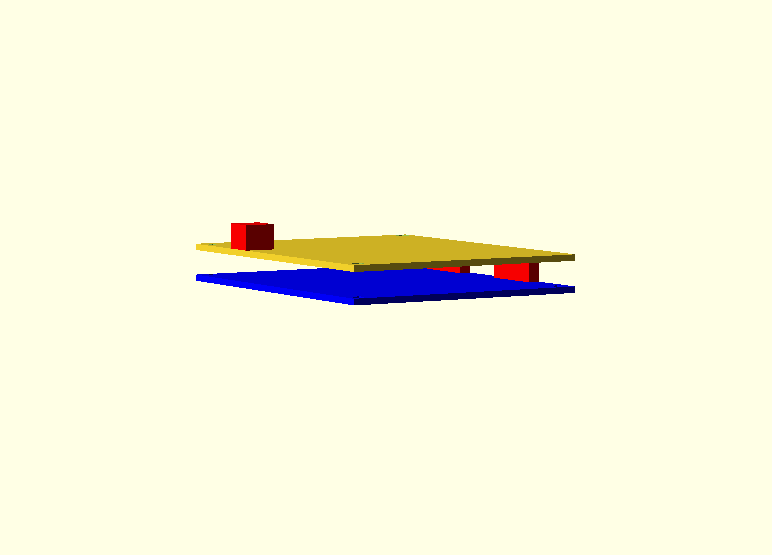
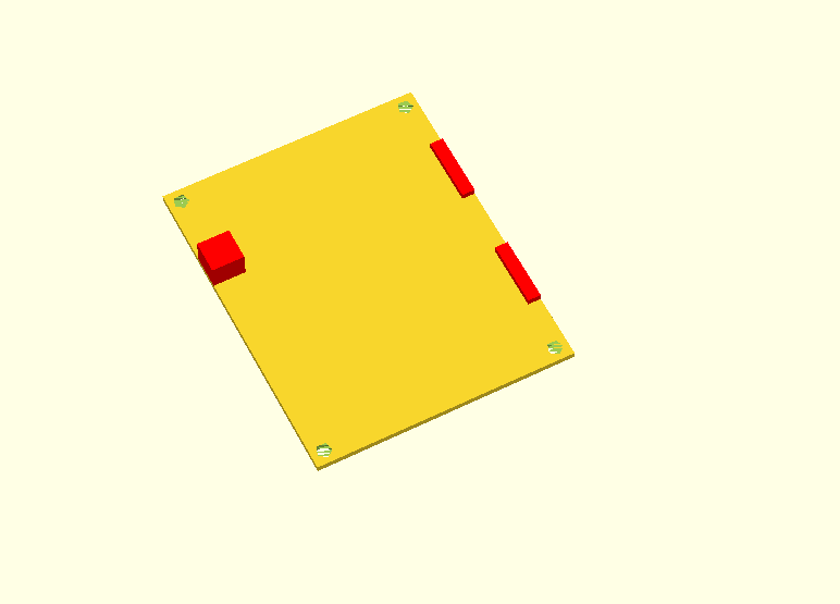
Shown below is a mock image of a v2 board with possible gigabit jack placement and rear IO and RF connectors.
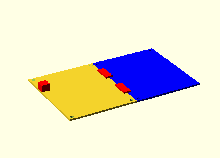
V2 will have a companion QRP PA board based on this work. This board must also be 100mm by 80mm. Shown below is a mock image of how this PA companion board will interface via 0.1 connectors to the v2 Hermes-Lite. In this configuration, a 100mm wide by 160mm deep extruded aluminum enclosure is required.
For v2 plus PA in flat orientation, this enclosure may be used.
The PA companion board must also have 4 holes, one at each corner, that align with a v2 Hermes-Lite hole. This allows for a tall sandwich configuration as seen below. Note that components such as the gigabit ethernet jack and filters will be facing out on each board. There can be no large components in the middle of the sandwich. Either the PA or v2 Hermes-Lite can be considered the top. Standoffs can be used to keep the board from resting on components.
For v2 plus PA in sandwich orientation, this enclousre will be the target.