-
Single-cycle CPU
-
Multi-cycle CPU
-
Pipelined CPU
-
Tomasulo CPU
Verilog is one of the Hardware Description Language (HDL) used to model the electronics systems at the following abstraction levels:
-
Register Transfer Level (RTL) - An abstraction level, where the circuits are modelled as the flow of data between registers. This is achieved through always blocks and assign statements. The RTL should be written in a way such that it is completely synthesizable, i.e., can be translated/synthesized to gate level
-
Behavioral - An abstraction level, which mimics the desired functionality of the hardware but is not necessarily synthesizable. Behavioral verilog is often used to represent analog block, place holder code, testbench code, and most importantly for modelling hardware for behavioral simulation.
-
Structural - Logic described by gates and modules only. No always blocks or assign statements. This is a representative of the real gates in the hardware.
Here, we will try to create exaples of hardware using RTL model and test it using an appropriate testbench.
The basic structure of code we will follow for hardware modelling the design is as follows:
module design_name (input <input_port_names>,
       output <output_port_names>);

       //internal registers and wires
       reg <reg_names>;
       wire <wire_names>;

       //combinational logic for next-state-logic
       always @ (*) begin
            //Combinational Statements using blocking assignments
       end

       //sequential logic for state-memory
       always @ (posedge clk) begin
            //Sequential Statements with non-blocking assignments
            //Reset statement necessary
       end

       //combinational logic for output-functional-logic
       assign <output_post_name> = <reg_name/wire_name>;
endmodule
The basic structure of code we will follow for creating a testbench to test the design is as follows:
module design_name_tb ();

       //internal registers and wires
       reg <reg_names>;     // All design inputs should be registers
       wire <wire_names>;   // All design outputs can be wires

       //initialize the design
       design_name <instant_name> (.input_port_names(reg_names), .output_port_names(wire_names));

       //If the design has clock, create a clock (here clock period = 2ns)
       always #1 clk = ~clk

       //test vectors input
       initial begin
              // initialize all inputs to initial values

              // write the input vectors here

              #5 $stop; //terminate the simulation
       end
endmoduleThe latch is modelled in verilog as
module d_latch (input en, d,
                output q);
    always @ (*) begin
        if (clk)
            q = d;
    end
endmodule
However, sometines a latch can be inferred in a verilog code unexpectedly due to incorrect coding practice such as when a combinational logic has undefined states. These can be -
-
Signal missing in the sensitivity list
always @(a or b)
begin
  out = a + b + c;  // Here, a latch is inferred for c,
                    // since it is missing from sensitivity list
end
-
Coverage not provided for all cases in an if-statement or case-statement
In the following case , we have a case where q = d for en = 1. However, the tool does not know what to do when en = 0, and infers a latch
always @(d or q)
begin
  if (en) q = d;    // Condition missing for en = 0; previous value
  	  	      // will be held through latch
end
Similarly, in the following case, if default case is missing in case statement and we don't have coverage for all possible cases, a latch is inferred.
always @(d or q)
begin
     case (d)
   	  2'b00: q = 0;
   	  2'b01: q = 1;
   	  2'b10: q = 1; // default condition missing; latch will be
   			// inferred for condition d = 2'b11 to hold the
   			// previous value
     endcase
end
Note: Latches are only generated by combinational always blocks, the sequential always block will never generate a latch.
The half adder circuit is realized as shown in Figure 1. The block has two inputs a & b, and two outputs sum and cout

The same can be written in verilog as -
module half_adder (input a, b,
		      output sum, cout);
 	assign sum = a ^ b;
 	assign cout = a & b;
endmodule
module full_adder (input a, b,
output sum, cout);
assign {cout, sum} = a + b;
endmoduleThe half adder circuit is realized as shown in Figure 1. The block has two inputs a, b & cin, and two outputs sum and cout
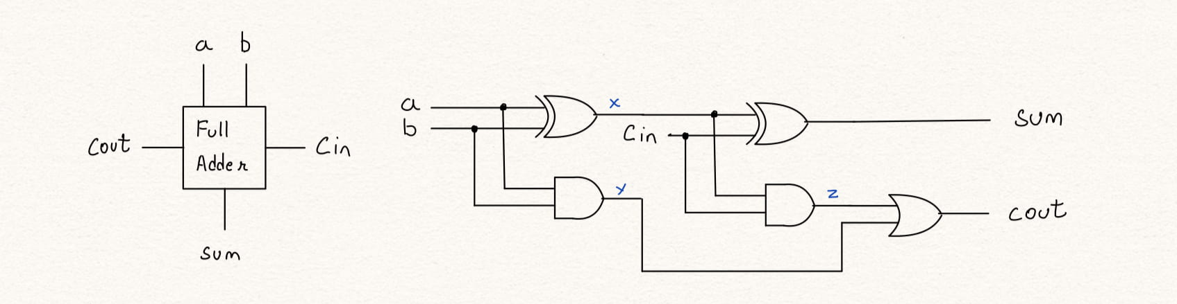
The same can be written in verilog in many different ways-
module full_adder (input a, b, cin,
		      output sum, cout);
 	wire x, y, z;
 	assign x = a ^ b;
 	assign sum = x ^ cin;
 	assign y = a & b;
 	assign z = x & cin;
 	assign cout = y | z;
endmodule
module full_adder (input a, b, cin,
output sum, cout);
assign {cout, sum} = a + b + cin;
endmodulemodule full_adder (input a, b, cin,
output sum, cout);
assign sum = a ^ b ^ cin;
assign cout = (a & b) | ((a ^ b) & cin);
endmodule
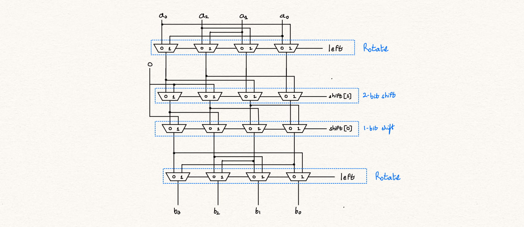

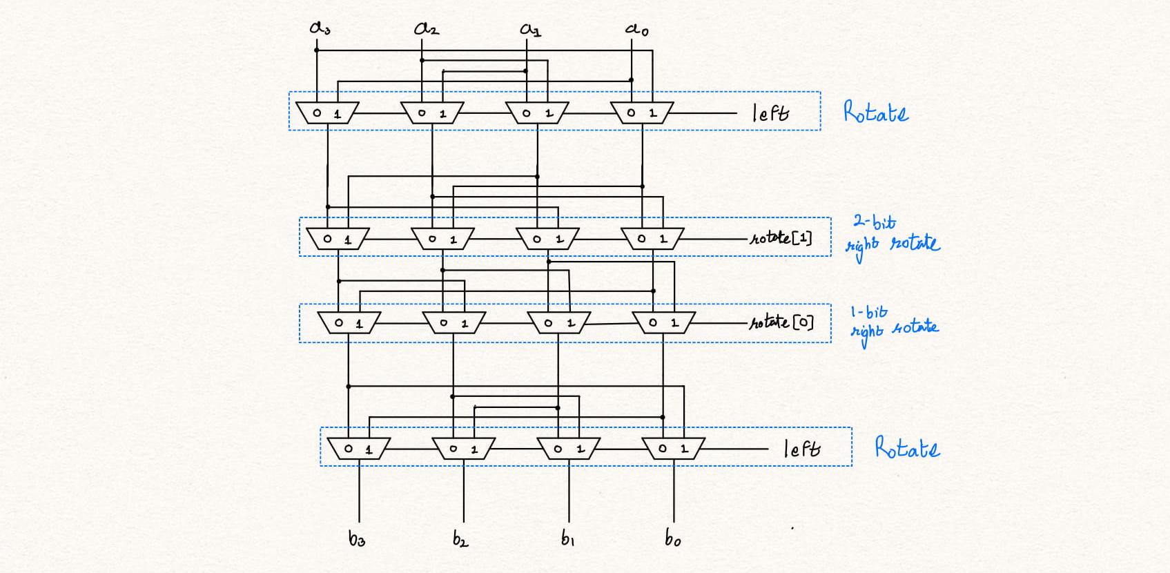
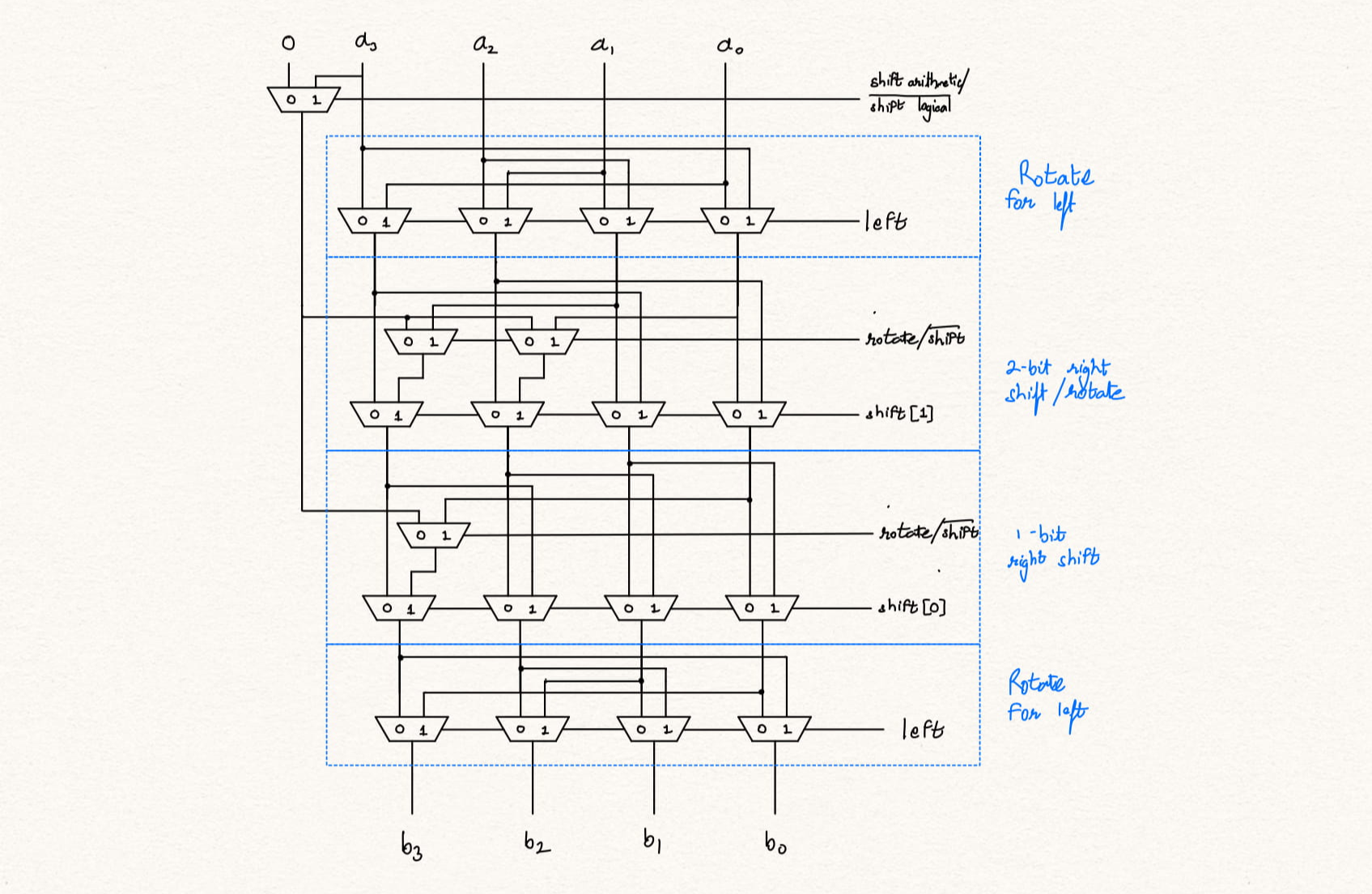
Additional information can be found at Design alternatives for barrel shifters

Sorting is a very important task generally performed through software, however, in hing sorting demand operations such as artificial intelligence and databases it becomes a necessity to implement sorting through hardware to speedup the process. This is implemented in hardware through a basic building block called compare and swap (CAS) block. The CAS block is connected in a certain way called bitonic network to sort the given set of numbers.
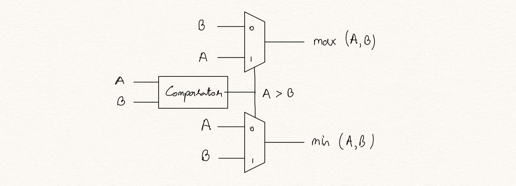
Figure 1: Compare and Swap Block
The CAS block has two inputs, A and B and has two outputs O1 = max(A,B) and O2 = min(A,B). A CAS block is made up of an n-bit comparator, two n-bit multiplexers to select from inputs A and B where n-bit is the data width of A and B. There can be two configurations of the CAS block to sort the numbers in an ascending or descending order.
To differentiate between the ascending and decending order CAS blocks, we use arrows to depict the type of sort. The arrow-head indicates port with max output and the arrow-root indicates the port with the min output.
module comapre_and_swap(input [3:0] data1, data2,
                        output [3:0] max, min);

  // Comparator output declaration
  wire data1_greater_than_data2;

  // Comparator output = 1 if data1 > data2
  // Comparator output = 0 if data1 <= data2
  assign data1_greater_than_data2 = data1 > data2;

  // max data
  assign max = (data1_greater_than_data2 == 1'b1) ? data1 : data2;

  // min data
  assign min = (data1_greater_than_data2 == 1'b1) ? data2 : data1;

endmodule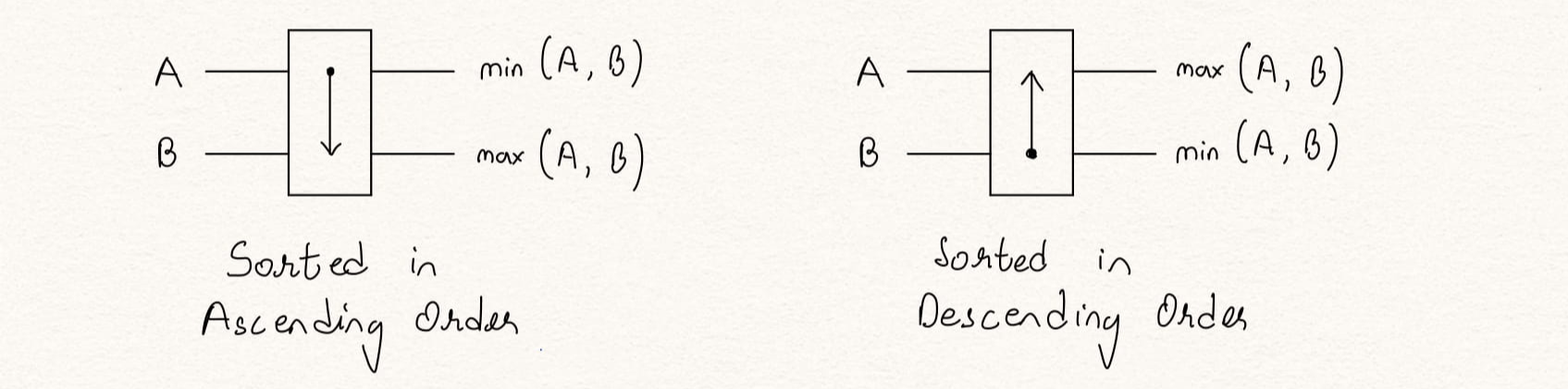
Figuren 2: Ascending and descending CAS blocks
A sorting network is a combination of CAS blocks, where each CAS block takes two inputs and swaps it if required, based on its ascending or descending configuration. Bitonic sorting networks uses the procedure of bitonic merge (BM), given two equal size sets of input data, sorted in opposing directions, the BM procedure will create a combined set of sorted data. It recursively merges an ascending and a descending set of size N /2 to make a sorted set of size N. Figure 3 and Figure 4 shows the CAS network for a 4-input and 8-input bitonic sorting network made up of ascending and descending BM units.
The total number of CAS blocks in any N-input bitonic sorting is N × log2 ( N ) × (log2( N ) + 1)/4. The following table shows the CAS blocks needed for N-input bitonic networks.
| Input data numbers | 8 | 16 | 32 | 256 |
|---|---|---|---|---|
| CAS blocks needed in sorting network | 24 | 80 | 240 | 4608 |
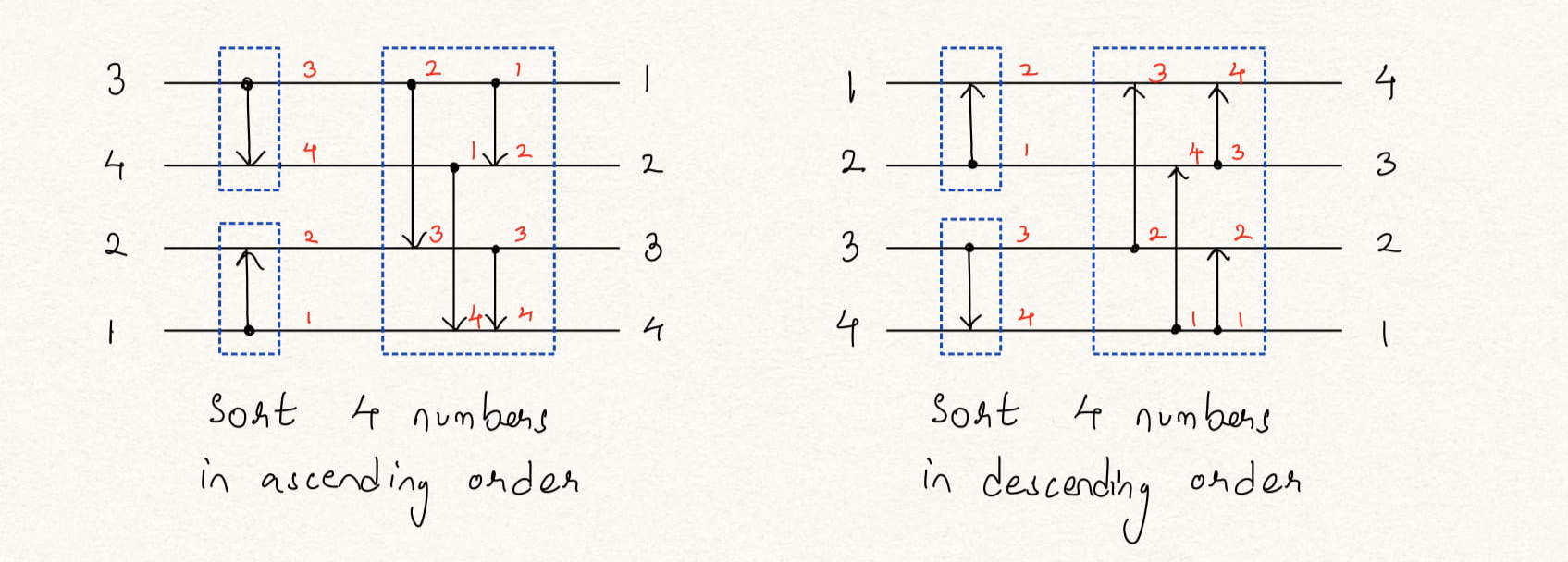
Figure 3: Sorting 4 numbers using CAS blocks in ascending and descending order
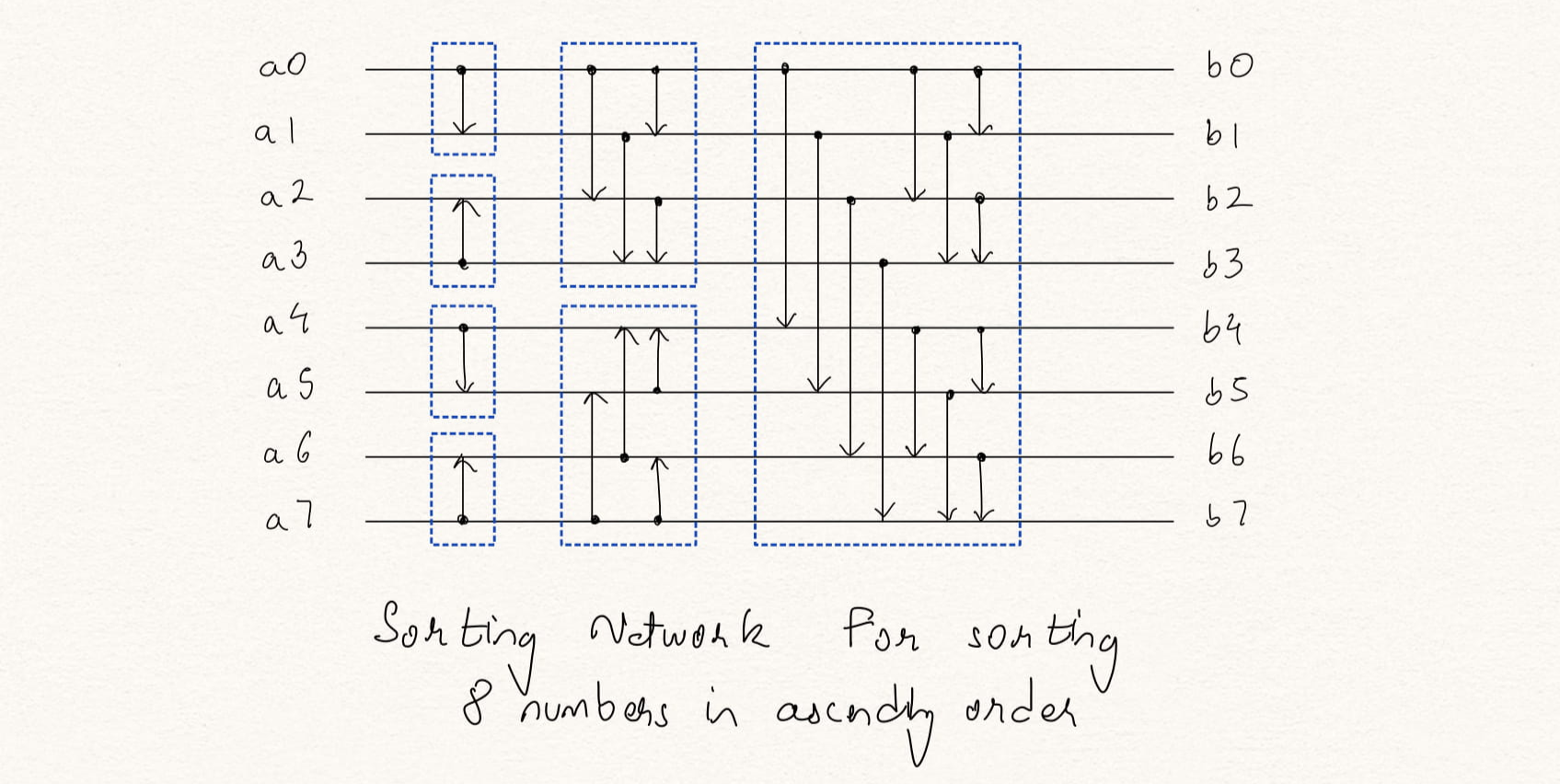
Figure 4: Sorting 8 numbers using CAS blocks in ascending order
module sort_network_8x4 (input [3:0] data_in [0:7],
                         output [3:0] data_sort [0:7]);

  // wire declarations for all the sorting intermediaries
  wire [3:0] stage1 [0:7];

  wire [3:0] stage2_0 [0:7];
  wire [3:0] stage2_1 [0:7];

  wire [3:0] stage3_0 [0:7];
  wire [3:0] stage3_1 [0:7];
  wire [3:0] stage3_2 [0:7];


  //------------------------------------------------------------------------
  // Stage 0 has only one level of sorting
  //------------------------------------------------------------------------
  comapre_and_swap u1 (data_in[0], data_in[1], stage1[1], stage1[0]);
  comapre_and_swap u2 (data_in[2], data_in[3], stage1[2], stage1[3]);
  comapre_and_swap u3 (data_in[4], data_in[5], stage1[5], stage1[4]);
  comapre_and_swap u4 (data_in[6], data_in[7], stage1[6], stage1[7]);

  //------------------------------------------------------------------------
  //Stage 1 has 2 levels of sorting
  //------------------------------------------------------------------------
  comapre_and_swap u5 (stage1[0], stage1[2], stage2_0[2], stage2_0[0]);
  comapre_and_swap u6 (stage1[1], stage1[3], stage2_0[3], stage2_0[1]);
  comapre_and_swap u7 (stage1[4], stage1[6], stage2_0[4], stage2_0[6]);
  comapre_and_swap u8 (stage1[5], stage1[7], stage2_0[5], stage2_0[7]);

  comapre_and_swap u9 (stage2_0[0], stage2_0[2], stage2_1[2], stage2_1[0]);
  comapre_and_swap u10 (stage2_0[1], stage2_0[3], stage2_1[3], stage2_1[1]);
  comapre_and_swap u11 (stage2_0[4], stage2_0[6], stage2_1[4], stage2_1[6]);
  comapre_and_swap u12 (stage2_0[5], stage2_0[7], stage2_1[5], stage2_1[7]);

  //------------------------------------------------------------------------
  // Stage 2 has 3 levels of sorting
  //------------------------------------------------------------------------
  comapre_and_swap u13 (stage2_1[0], stage2_1[4], stage3_0[4], stage3_0[0]);
  comapre_and_swap u14 (stage2_1[1], stage2_1[5], stage3_0[5], stage3_0[1]);
  comapre_and_swap u15 (stage2_1[2], stage2_1[6], stage3_0[6], stage3_0[2]);
  comapre_and_swap u16 (stage2_1[3], stage2_1[7], stage3_0[7], stage3_0[3]);

  comapre_and_swap u17 (stage3_0[0], stage3_0[2], stage3_1[2], stage3_1[0]);
  comapre_and_swap u18 (stage3_0[1], stage3_0[3], stage3_1[3], stage3_1[1]);
  comapre_and_swap u19 (stage3_0[4], stage3_0[6], stage3_1[6], stage3_1[4]);
  comapre_and_swap u20 (stage3_0[5], stage3_0[7], stage3_1[7], stage3_1[5]);

  comapre_and_swap u21 (stage3_1[0], stage3_1[1], stage3_2[1], stage3_2[0]);
  comapre_and_swap u22 (stage3_1[2], stage3_1[3], stage3_2[3], stage3_2[2]);
  comapre_and_swap u23 (stage3_1[4], stage3_1[5], stage3_2[5], stage3_2[4]);
  comapre_and_swap u24 (stage3_1[6], stage3_1[7], stage3_2[7], stage3_2[6]);

  // Sorted data is assigned to output
  assign data_sort = stage3_2;

endmodule
The information found here was referred from an outstanding paper Low-Cost Sorting Network Circuits Using Unary Processing
Additional information about sorting networks can be found here and here
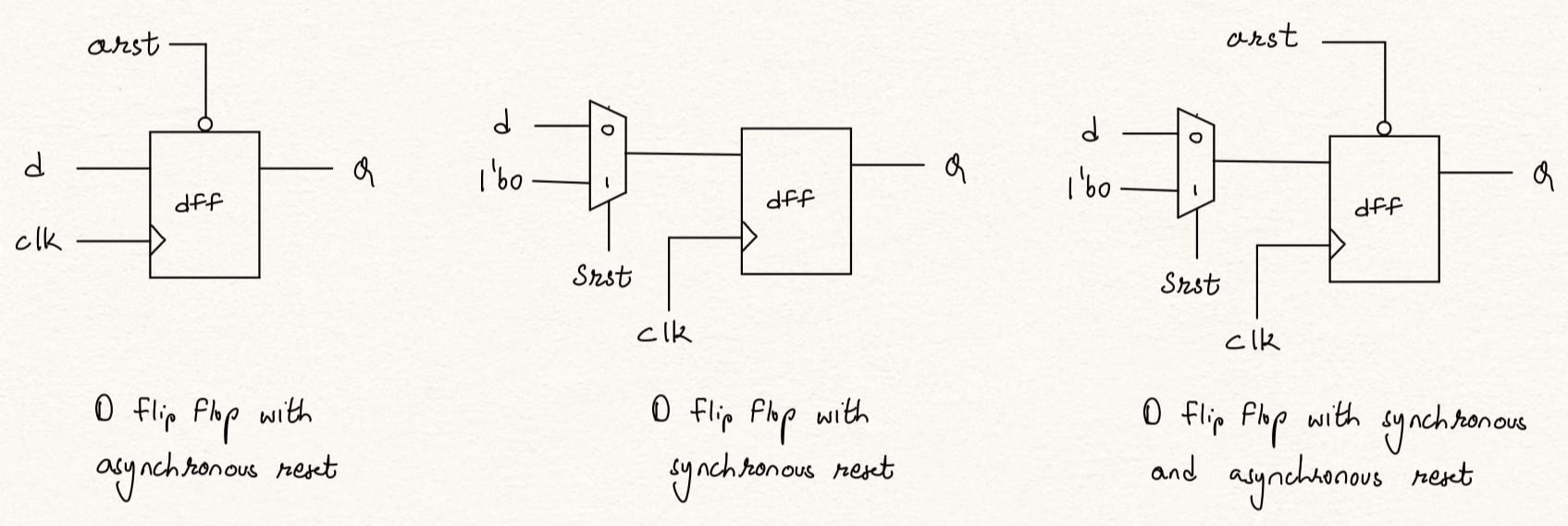
Verilog code for D flip-flop with active-high synchronous reset -
module dff (input d, clk, srst,
	    output reg Q);
    always @ (posedge clk) begin
        if (srst)
            Q <= 1'b0;
	else
	    Q <= d;
    end
endmodule
Verilog code for D flip-flop with active-low asynchronous reset -
module dff (input D, clk, arst,
	    output reg Q);
    always @ (posedge clk or negedge arst) begin
        if (~arst)
            Q <= 1'b0;
	else
	    Q <= D;
    end
endmodule
Verilog code for D flip-flop with active-low asynchronous reset -
module dff (input D, clk, arst, srst
	    output reg Q);
    always @ (posedge clk or negedge arst) begin
        if (~arst)
            Q <= 1'b0;
	else if (srst)
	    Q <= 1'b0;
	else
	    Q <= D;
    end
endmodule
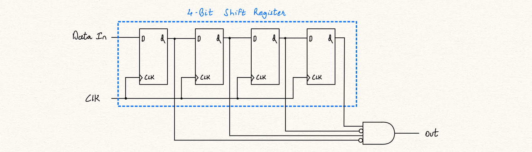
Typically in a Serial in Parallel out circuit, there are as many flops as the size of the parallel out. The input data is shifted in with clk and when all the data bits are available, the serially loaded data is read through the parallel port.
Here, say we have 8-bit parallel port, so it takes 8 clk cycles to serially load 8-bits of data and the data is available for 1 clock cycle and then new data starts coming in resulting in the output being stable for only 1 clock cycle.
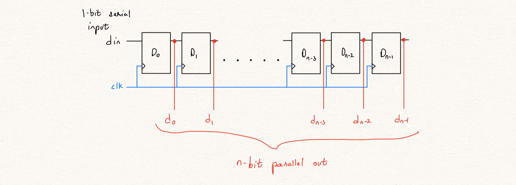
Figure 1: Basic serial-in-parallel-out circuit
module sipo_1 (input load, clk, rst,
               input data_in,
               output [7:0] data_out);

  // SIPO register array to read and shift data
  reg [7:0] data_reg;

  always @ (posedge clk or negedge rst) begin
    if (~rst)
      data_reg <= 8'h00; // Reset SIPO register on reset
    else if (load)
      data_reg <= {data_in, data_reg[7:1]}; // Load data to the SIPO register by right shifts
  end

  // Assign the SIPO register data to data_out wires
  assign data_out = data_reg;

endmodule
If there is a need to keep the output data stable until we have the next valid data, we need to use a 2-step architecture as shown below. The data is clocked in to the serial registers at the serial_clk then when valid data is loaded, the serial_clk and parallel_clk are asserted together. This way the data loaded into the output registers stay constant until the next valid data is loaded serially.
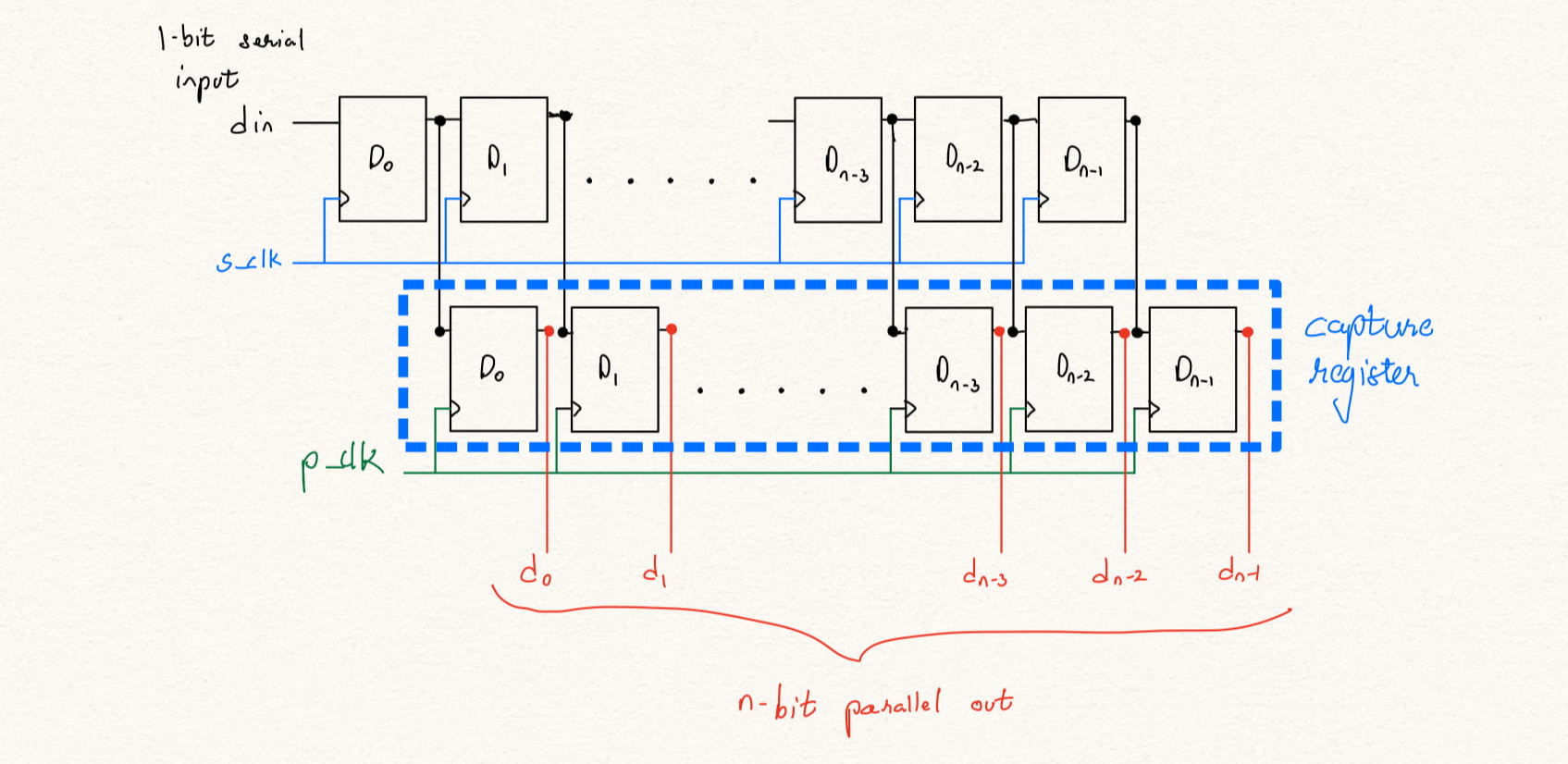
Figure 2: Serial-in-parallel-out circuit with capture register
module sipo_2 (input load, clk, rst,
               input data_in,
               output reg [7:0] data_out);

  // SIPO register array to read and shift data
  reg [7:0] data_reg;

  always @ (posedge clk or negedge rst) begin
    if (~rst) begin
      data_reg <= 8'h00; // Reset SIPO register on reset
      data_out <= 8'h00; // Reset capture register
    end
    else begin
      if (load)
        data_reg <= {data_in, data_reg[7:1]}; // Load data to the SIPO register by right shifts
      else
        data_out <= data_reg; // Assign SIPO register data to capture register
    end
  end

endmodule
Parallel-in serial-out is a one of the basic elements of serializer-deserializer (SerDes) circuits. The PISO allows the parallel loading of data following which the data can be shifted out serially from either the MSB or the LSB side. This is how a parallel to serial conversion takes place.

To load the data we need as many flip-flops as the data width of the parallel loading, i.e., if the data width is 8 bits, we need 8 flip flops to store these 8 bits. To differentiate between a load or shift operation we need an additional input which can be multiplexed for indicating either shift and load. If the signal is 1 it indicates a load and if 0 a shift.
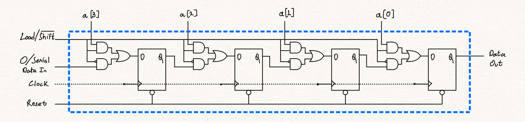
The loading can be be asynchronous needing a flip-flop with set/reset pins. However, here we will be looking at a circuit with synchronous loading and shifting of 4-bit data
module piso (input load, clk, rst,
             input [7:0] data_in,
             output reg data_out);

  // PISO register array to load and shift data
  reg [7:0] data_reg;

  always @ (posedge clk or negedge rst) begin
    if (~rst)
      data_reg <= 8'h00; // Reset PISO register array on reset
    else begin

      // Load the data to the PISO register array and reset the serial data out register
      if (load)
      	{data_reg, data_out} <= {data_in, 1'b0};
      // Shift the loaded data 1 bit right; into the serial data out register
      else
      	{data_reg, data_out} <= {1'b0, data_reg[7:0]};
    end
  end

endmodule
The gray code is a type of binary number ordering such that each number differes from its previous and the following number by exactly 1-bit. Gray codes are used in cases when the binary numbers transmitted by a digital system may result in a fault or ambuiguity or for implementing error corrections.
The most simple implementation of a gray code counter will be a binary counter followed by a binary to gray converter. However, the datapath is huge resulting in a very low clock frequency. This is a good motive to pursue a design to implement a gray counter with a smaller datapath.

Consider a 4-bit gray code gray[3:0] in the following table.
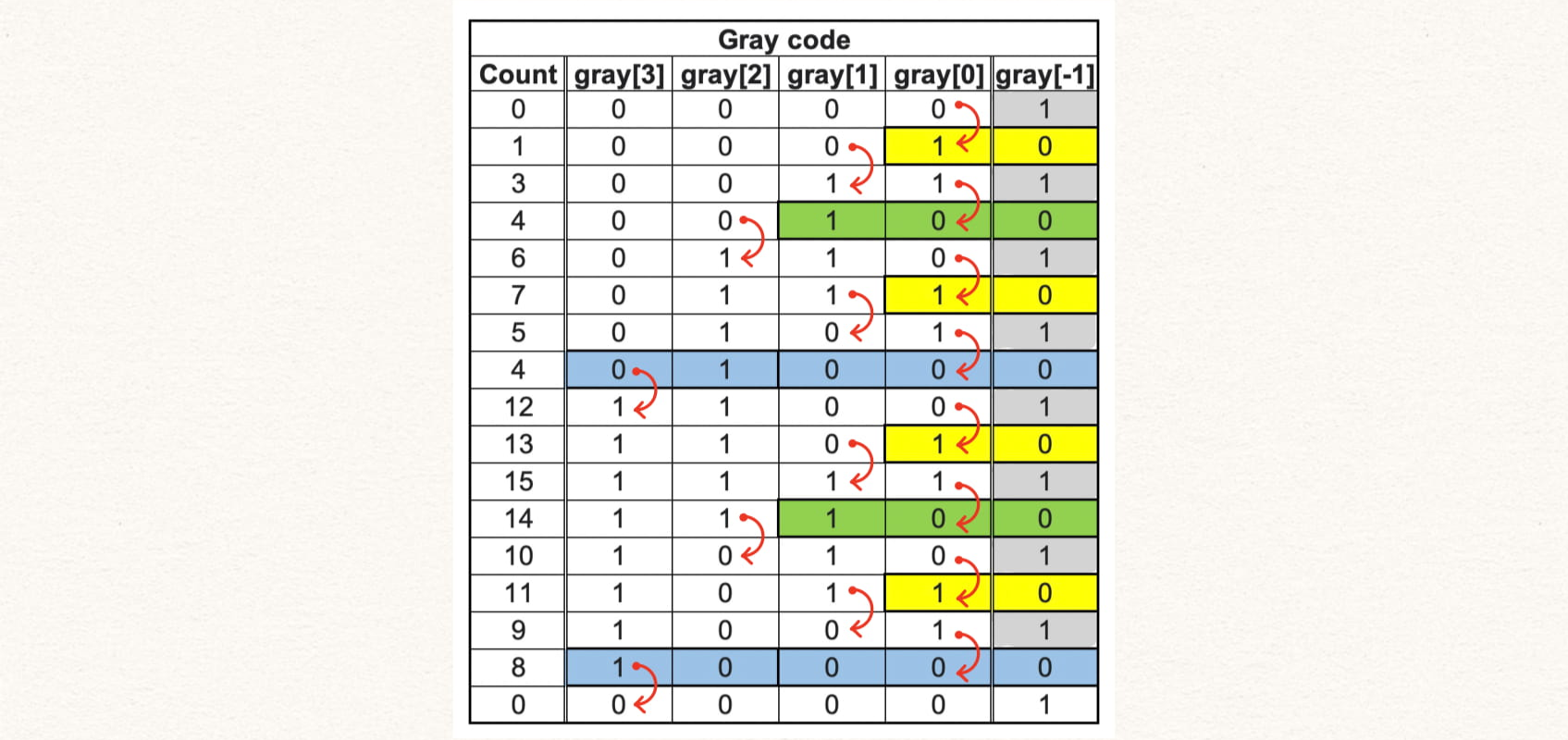
The count column gives the decimal value for the corrseponding gray code, gray[3:0] represent the binary encoded gray code, and gray[-1] is a place-holder and used to actually implement the gray code counter.
From the table the following observations can be made -
- gray[-1] flips every clock cycle, and is preset to
1'b1 - gray[0] flips everytime
gray[-1] == 1 - gray[1] flips everytime
(gray[0] == 1) & (gray[-1] == 0) - gray[2] flips everytime
(gray[1] == 1) & (gray[0] == 0) & (gray[-1] == 0) - gray[3] flips twice for a cycle which means we need additional condition to account for this. It flips when and
(gray[3] == 1) or (gray[2] == 0)and(gray[1] == 0) & (gray[0] == 0) & (gray[-1] == 0)
The red arrow in the table shows the bit getting flipped and the highlighed bits show the condition for the flip.
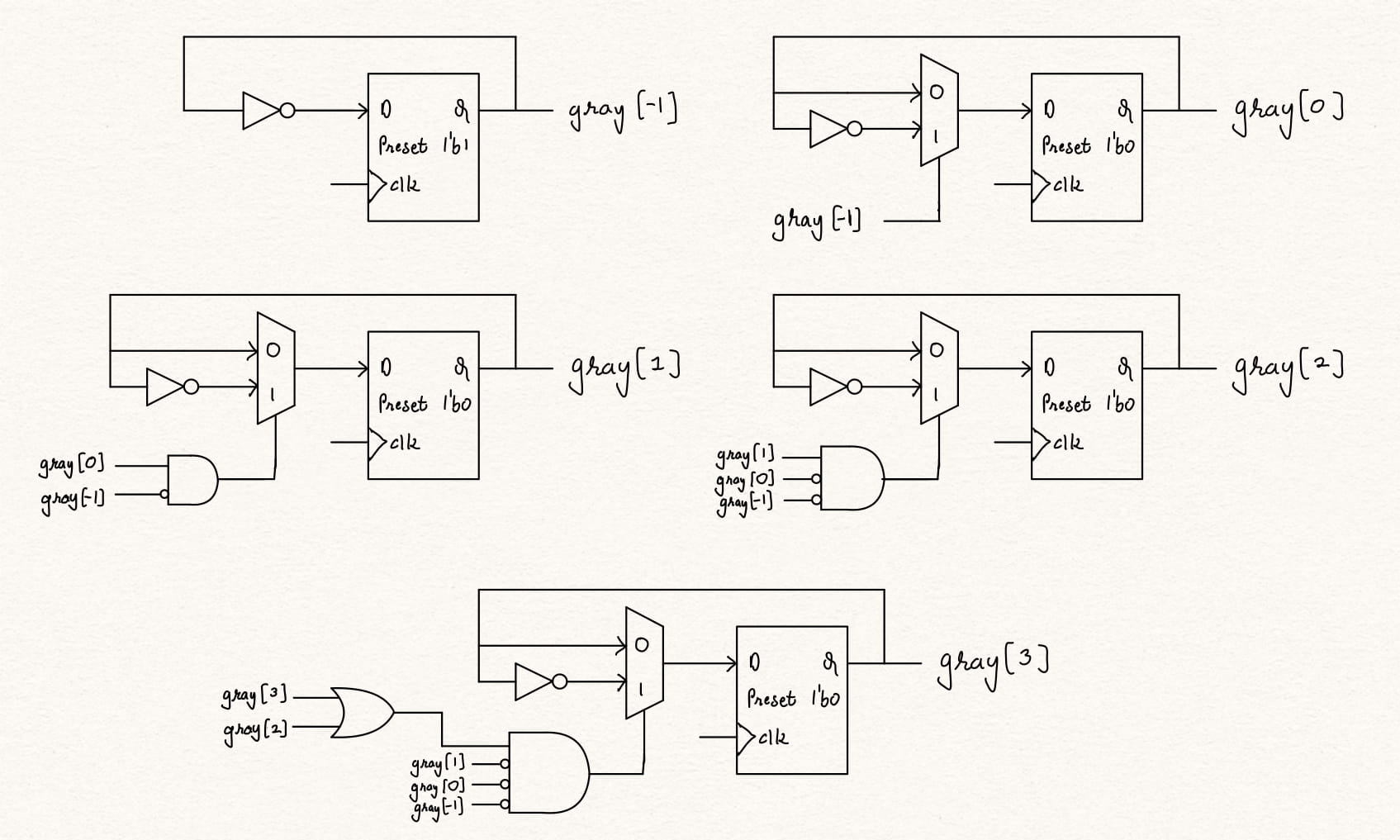
The same has been shown here in the following circuit. gray[3:-1] is represented by the flip-flops and the logic when these flip make up the combinational logic.
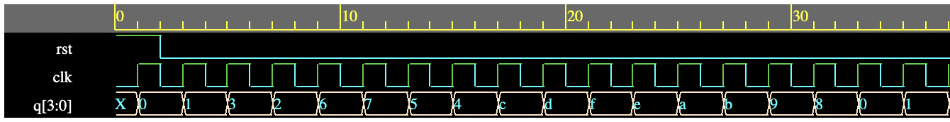
module gray_counter(input clk, rst,
                    output [3:0] gray_count);

  // D flip flops to store the gray count and the placeholder value
  reg [3:-1] q;

  // register declaration for combinational logic
  reg all_zeros_below[2:-1];

  // Combinational logic to compute if the value below any bit of the gray count is 0
  always @ (*) begin
    all_zeros_below[-1] = 1;
    for (integer i = 0; i<3; i= i+1) begin
      all_zeros_below[i] = all_zeros_below[i-1] & ~q[i-1];
    end
  end

  always @ (posedge clk) begin
    if (rst) q[3:-1] <= 5'b0000_1;

    else begin
      // The placegolder value toggles every clock
      q[-1] <= ~q[-1];

      // The bits [n-1:0] toggle everytime the sequence below it is 1 followed by all zeros (1000...)
      for (integer i = 0; i<3; i= i+1) begin
        q[i] <= (q[i-1] & all_zeros_below[i-1]) ? ~q[i] : q[i];
      end

      // The MSB flips when either the nth/(n-1)th bit is 1 followed by all zeros (X1000... or 1X000...)
      q[3] <= ((q[3] | q[2]) & all_zeros_below[2]) ? ~q[3] : q[3];
    end
  end

  // The flip flop value is connected to the gray counter output.
  assign gray_count = q[3:0];

endmodule
The Fibonacci numbers together form a fibonacci sequence, F(n), such that each number is the sum of the two preceding ones, starting from 0 and 1
i.e., F(0) = 0, F(1) = 1
and F(n) = F(n-1) + F(n-1) for all n > 2
The Fibonacci sequence thus becomes, 0, 1, 1, 2, 3, 5, 8, 13, 21, ....
The fibonacci numbers are used in various computational applications involving hardware:
- Pseudorandom number generators
- Determining the greatest common divisor
- A one-dimensional optimization method, called the Fibonacci search technique
- The Fibonacci number series is used for optional lossy compression
Instead of performing the fibonacci computation using software which consumes a lot of time it is easier to faster to implement the fibonacci counter in hardware.
Fibonacci Counter can be implemented in hardware with two registers A and B to store the initial numbers in the series, i.e., A = 1 and B = 0. The sum of the both A and B can be stored in A and the value in A can be moved into B and register B is used as the output. However, in the 2 register format, after reset we don't see the initial sequence number '0'. This can be resolved by adding a register C in series. The same is shown in the following waveform and schematic.
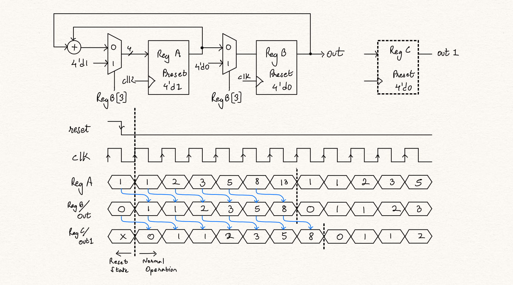
The same can be implemented in verilog as -
module fibC (input clk, rst,
            output [3:0] out);

  // Registers to store the current and previous values of the fibonacci counter
  reg [3:0] RegA, RegB, RegC;

  always @ (posedge clk) begin
    if (rst) begin
      RegA <= 4'h1;	// Start RegA with the second value of fibonacci series - '1'
      RegB <= 4'h0;	// Start RegB with the first value of fibonacci series - '0'
      RegC <= 4'h0; // Reset RegC to '0'
    end
    else begin
      RegA <= RegB[3] ? 4'h1 : RegA + RegB; // if RegB == 8, reset RegA
      RegB <= RegB[3] ? 4'h0 : RegA;	// if RegB == 8, reset RegB
      RegC <= RegB;	// RegC is a synchronization register
    end
  end

  // Only one of the following two lines should be uncommented

  assign out = RegB;	// To ignore the '0' at the startup after reset, uncomment this line
  //assign out = RegC;	// To start with a '0' at startup after reset, uncomment this line

endmodule

Frequency divider is any curcuit that divides the frequency of the input signal, say f by a factor n, such that the frequency of the output signal is f/n. The frequency dividers with uneven pulse widths are very simple to be implemented with the use of counters and mod-n counters discussed earlier. However, we need additional circuitry to create a frequency divider with 50% duty cycle.
Here, all the following frequency dividers have integer dividers n = 1,2,3,4,5.... and have a 50% duty cycle.
The most basic a 1-bit counter also doubles up as a divide-by-2 circuit since for any given clock frequency, the output of the 1 bit counter is 1/2 the frequency of the cock signal.

The same can be modelled in verilog as:
module div_by_2 (input clk, rst,
                 output clk_out);

  // Register to store the current count value
  reg Q;

  // State memory
  always @ (posedge clk) begin
    if (rst)
      Q <= 1'b0;	// If reset, set Q to 0
    else
      Q <= ~Q;		// If not reset, set Q to the next count value
  end

  // The clk/2 is set when Q == 1
  assign clk_out = Q;
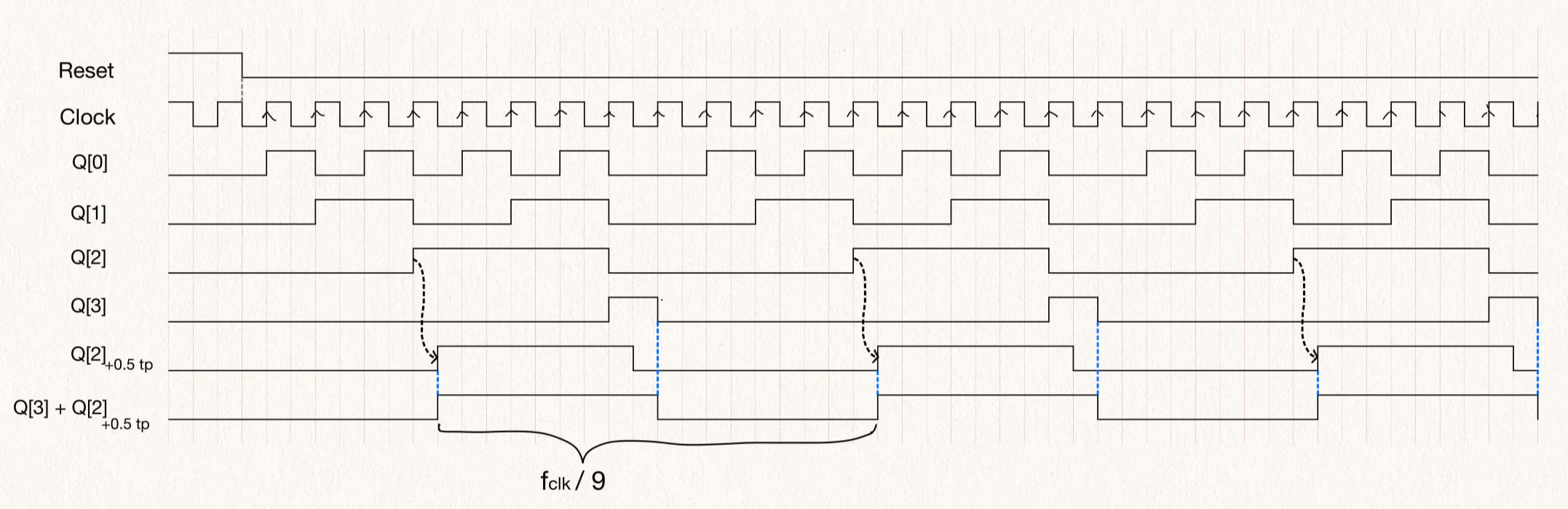
endmodule To implement a divide by 3, we need to count to 3 and so we will need two flip-flops to count states 2'b00, 2'b01, 2'b10. However since dividing factor is not equal to 2^n we need additional flip-flops to get a 50% duty-cycle. We can achieve this by shifting the state Q[0] by 1/2 clock cycle and then ORing with Q[1]. The 1/2 clock cycle shift is made by using a negative edge-triggered flip-flop.
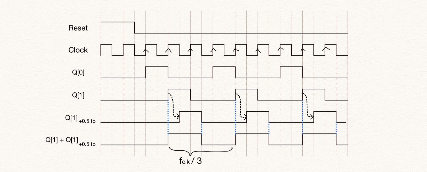
Here, tp stands for time period of the clock, i.e. + 0.5 tp stands for the signal delayed by 0.5 clock period.
The same can be modelled in verilog as:
module div_by_3 (input clk, rst,
                 output clk_out);

  // Registers to store the current count value and wire to compute the next count value
  reg [1:0] Q, Q_next;

  // Register to delay Q[0] signal by 0.5 clock period
  reg Q_delay_0_5tp;

  // Combinational logic to compute the next state logic (count value)
  always @ (*) begin
    case(Q)
      2'b00: Q_next = 2'b01;
      2'b01: Q_next = 2'b10;
      2'b10: Q_next = 2'b00;
      default: Q_next = 2'b00;
    endcase
  end

  // State memory
  always @ (posedge clk) begin
    if (rst)
      Q <= 2'h0;	// If reset, set Q to 0
    else
      Q <= Q_next;	// If not reset, set Q to the next count value
  end

  // Always block to delay Q[0] by 0.5 clock cycle
  always @ (negedge clk) begin
    if (rst)
      Q_delay_0_5tp <= 1'b0;
    else
      Q_delay_0_5tp <= Q[0];
  end

  // The clk/3 is set when Q[0]_delayed_by_0.5_cycle == 1 or Q[1] == 1
  assign clk_out = Q_delay_0_5tp | Q[1];
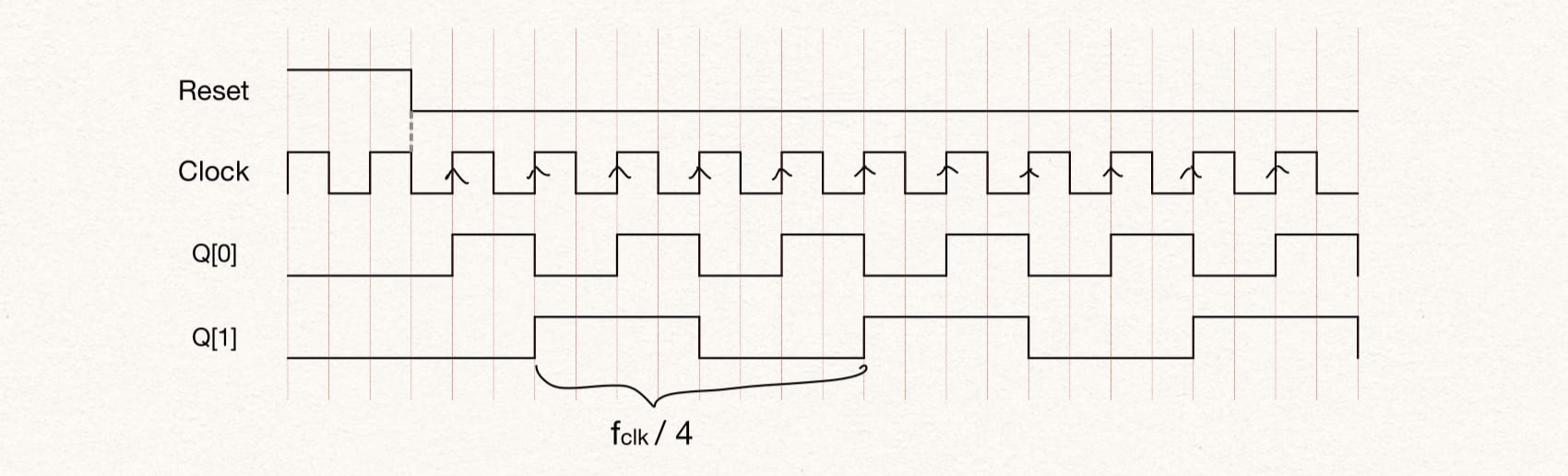
endmoduleTo implement a divide by 4, we need to count to 4 and so we will need two flip-flops to count states 2'b00, 2'b01, 2'b10, 2'b10. We can use the state Q[1] as the output which has the frequency fclk/4.
module div_by_4 (input clk, rst,
                 output clk_out);

  // Registers to store the current count value and wire to compute the next count value
  reg [1:0] Q, Q_next;

  // Combinational logic to compute the next state logic (count value)
  always @ (*) begin
    case(Q)
      2'b00: Q_next = 2'b01;
      2'b01: Q_next = 2'b10;
      2'b10: Q_next = 2'b11;
      2'b11: Q_next = 2'b00;
      default: Q_next = 2'b00;
    endcase
  end

  // State memory
  always @ (posedge clk) begin
    if (rst)
      Q <= 2'h0;	// If reset, set Q to 0
    else
      Q <= Q_next;	// If not reset, set Q to the next count value
  end

  // The clk/4 is set when Q[1] == 1
  assign clk_out = Q[1];

endmoduleTo implement a divide by 5, we need to count to 3 and so we will need 3 flip-flops to count states 2'b000, 2'b001, 2'b010, 2'b011, 2'b100. However since dividing factor is not equal to 2^n we need additional flip-flops to get a 50% duty-cycle. We can achieve this by shifting the state Q[1] by 1/2 clock cycle and then ORing with Q[2]. The 1/2 clock cycle shift is made by using a negative edge-triggered flip-flop.

The table shows the current counter state and the next state. The first column shows the clock divider output. It must be noted the 0/1 and 1/0 refers to the signal changing from 0 -> 1 and 1 -> 0 respectively at the falling edge of the clock.
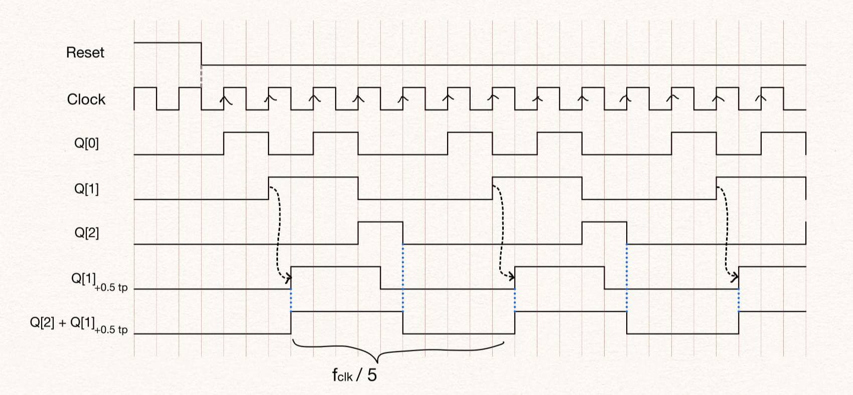
Here, tp stands for time period of the clock, i.e. + 0.5 tp stands for the signal delayed by 0.5 clock period.
The same can be modelled in verilog as:
module div_by_5 (input clk, rst,
                 output clk_out);

  // Registers to store the current count value and wire to compute the next count value
  reg [2:0] Q, Q_next;

  // Register to delay Q[1] signal by 0.5 clock period
  reg Q_delay_0_5tp;

  // Combinational logic to compute the next state logic (count value)
  always @ (*) begin
    if (Q == 3'd4)
      Q_next = 3'h0;	// If counted to 4, set Q to 0
    else
      Q_next = Q + 1; 	// If not counted to 4, set Q to Q + 1
  end

  // State memory
  always @ (posedge clk) begin
    if (rst)
      Q <= 3'h0;	// If reset, set Q to 0
    else
      Q <= Q_next;	// If not reset, set Q to the next count value
  end

  // Always block to delay Q[1] by 0.5 clock cycle
  always @ (negedge clk) begin
    if (rst)
      Q_delay_0_5tp <= 1'b0;
    else
      Q_delay_0_5tp <= Q[1];
  end

  // The clk/5 is set when Q[1]_delayed_by_0.5_cycle == 1 or Q[2] == 1
  assign clk_out = Q_delay_0_5tp | Q[2];

endmoduleTo implement a divide by 6, we need to count to 6 and so we will need 3 flip-flops to count states 2'b000, 2'b001, 2'b010, 2'b011, 2'b100, 2'b101. However since dividing factor is not equal to 2^n we need additional flip-flops to get a 50% duty-cycle. We can achieve this by shifting the state Q[1] by 1 clock cycle and then ORing with Q[2]. The 1 clock cycle shift is made by using a positive edge-triggered flip-flop.

The table shows the current counter state and the next state. The first column shows the clock divider output.
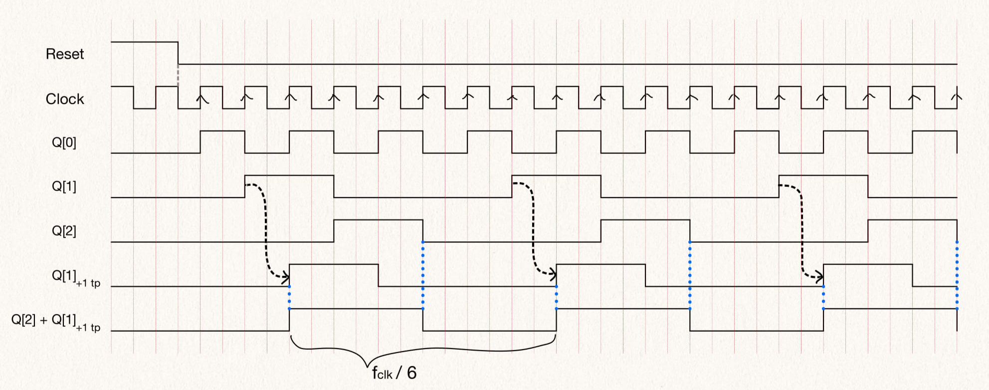
Here, tp stands for time period of the clock, i.e. + 1 tp stands for the signal delayed by 1 clock period.
The same can be modelled in verilog as:
module div_by_6 (input clk, rst,
                 output clk_out);

  // Registers to store the current count value and wire to compute the next count value
  reg [2:0] Q, Q_next;

  // Registers to delay Q[1] signal by 1 clock period
  reg Q_delay_1tp;


  // Combinational logic to compute the next state logic (count value)
  always @ (*) begin
    if (Q == 3'd5)
      Q_next = 3'h0;	// If counted to 5, set Q to 0
    else
      Q_next = Q + 1; 	// If not counted to 5, set Q to Q + 1
  end

  // State memory
  always @ (posedge clk) begin
    if (rst)
      Q <= 3'h0;	// If reset, set Q to 0
    else
      Q <= Q_next;	// If not reset, set Q to the next count value
  end

  // Always block to delay Q[1] by 1 clock cycle
  always @ (posedge clk) begin
    if (rst) begin
      Q_delay_1tp <= 1'b0;
    end
    else begin
      Q_delay_1tp <= Q[1];
    end
  end

  // The clk/6 is set when Q[1]_delayed_by_1_cycle == 1 or Q[2] == 1
  assign clk_out = Q_delay_1tp | Q[2];

endmoduleTo implement a divide by 9, we need to count upto 9 and so we will need two flip-flops to count states 4'b0000, 4'b0001, .... 4'b0111, 4'b1000. However since dividing factor is not equal to 2^n we need additional flip-flops to get a 50% duty-cycle. We can achieve this by shifting the state Q[2] by 1/2 clock cycle and then ORing with Q[3]. The 1/2 clock cycle shift is made by using a negative edge-triggered flip-flop.
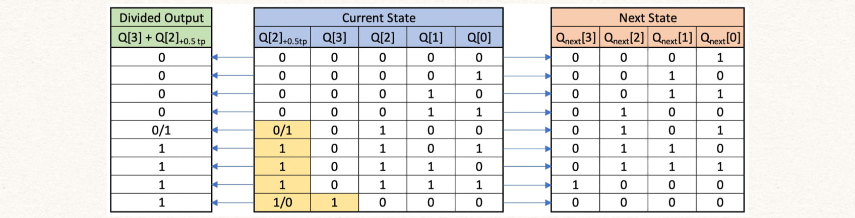
The table shows the current counter state and the next state. The first column shows the clock divider output. It must be noted the 0/1 and 1/0 refers to the signal changing from 0 -> 1 and 1 -> 0 respectively at the falling edge of the clock. All other values change at the rising edge of the clock.
Here, tp stands for time period of the clock, i.e. + 0.5 tp stands for the signal delayed by 0.5 clock period.
The same can be modelled in verilog as:
module div_by_9 (input clk, rst,
                 output clk_out);

  // Registers to store the current count value and wire to compute the next count value
  reg [3:0] Q, Q_next;

  // Register to delay Q[2] signal by 0.5 clock period
  reg Q_delay_0_5tp;

  // Combinational logic to compute the next state logic (count value)
  always @ (*) begin
    if (Q == 4'd8)
      Q_next = 4'h0;	// If counted to 8, set Q to 0
    else
      Q_next = Q + 1; 	// If not counted to 8, set Q to Q + 1
  end

  // State memory
  always @ (posedge clk) begin
    if (rst)
      Q <= 4'h0;	// If reset, set Q to 0
    else
      Q <= Q_next;	// If not reset, set Q to the next count value
  end


  // Always block to delay Q[2] by 1.5 clock cycle
  always @ (negedge clk) begin
    if (rst)
      Q_delay_0_5tp <= 1'b0;
    else
      Q_delay_0_5tp <= Q[2];
  end

  // The clk/9 is set when Q[2]_delayed_by_0.5_cycle == 1 or Q[3] == 1
  assign clk_out = Q_delay_0_5tp | Q[3];

endmoduleTo implement a divide by 11, we need to count upto 11 and so we will need two flip-flops to count states 4'b0000, 4'b0001, .... 4'b1001, 4'b1010. However since dividing factor is not equal to 2^n we need additional flip-flops to get a 50% duty-cycle. We can achieve this by shifting the state Q[2] by 1.5 clock cycles and then ORing with Q[3]. The 1.5 clock cycle shift is made by using a positive edge-triggered flip flop followed by a negative edge-triggered flip-flop.
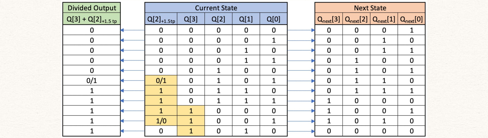
The table shows the current counter state and the next state. The first column shows the clock divider output. It must be noted the 0/1 and 1/0 refers to the signal changing from 0 -> 1 and 1 -> 0 respectively at the falling edge of the clock. All other values change at the rising edge of the clock.

Here, tp stands for time period of the clock, i.e. + 1.5 tp stands for the signal delayed by 1.5 clock periods.
The same can be modelled in verilog as:
module div_by_11 (input clk, rst,
                 output clk_out);

  // Registers to store the current count value and wire to compute the next count value
  reg [3:0] Q, Q_next;

  // Register to delay Q[2] signal by 1 clock period
  reg Q_delay_1tp;

  // Register to delay Q[2] signal by 1.5 clock period
  reg Q_delay_1_5tp;

  // Combinational logic to compute the next state logic (count value)
  always @ (*) begin
    if (Q == 4'd10)
      Q_next = 4'h0;	// If counted to 10, set Q to 0
    else
      Q_next = Q + 1; 	// If not counted to 10, set Q to Q + 1
  end

  // State memory
  always @ (posedge clk) begin
    if (rst)
      Q <= 4'h0;	// If reset, set Q to 0
    else
      Q <= Q_next;	// If not reset, set Q to the next count value
  end

  // Always block to delay Q[2] by 1 clock cycle
  always @ (posedge clk) begin
    if (rst)
      Q_delay_1tp <= 1'b0;
    else
      Q_delay_1tp <= Q[2];
  end

  // Always block to delay Q[2] by 1.5 clock cycle
  always @ (negedge clk) begin
    if (rst)
      Q_delay_1_5tp <= 1'b0;
    else
      Q_delay_1_5tp <= Q_delay_1tp;
  end

  // The clk/11 is set when Q[2]_delayed_by_1.5_cycle == 1 or Q[3] == 1
  assign clk_out = Q_delay_1_5tp | Q[3];

endmoduleTo implement a divide by 12, we need to count upto 12 and so we will need two flip-flops to count states 4'b0000, 4'b0001, .... 4'b1010, 4'b1011. However since dividing factor is not equal to 2^n we need additional flip-flops to get a 50% duty-cycle. We can achieve this by shifting the state Q[2] by 2 clock cycles and then ORing with Q[3]. The 1/2 clock cycle shift is made by using a 2 positive edge-triggered flip-flops in series.
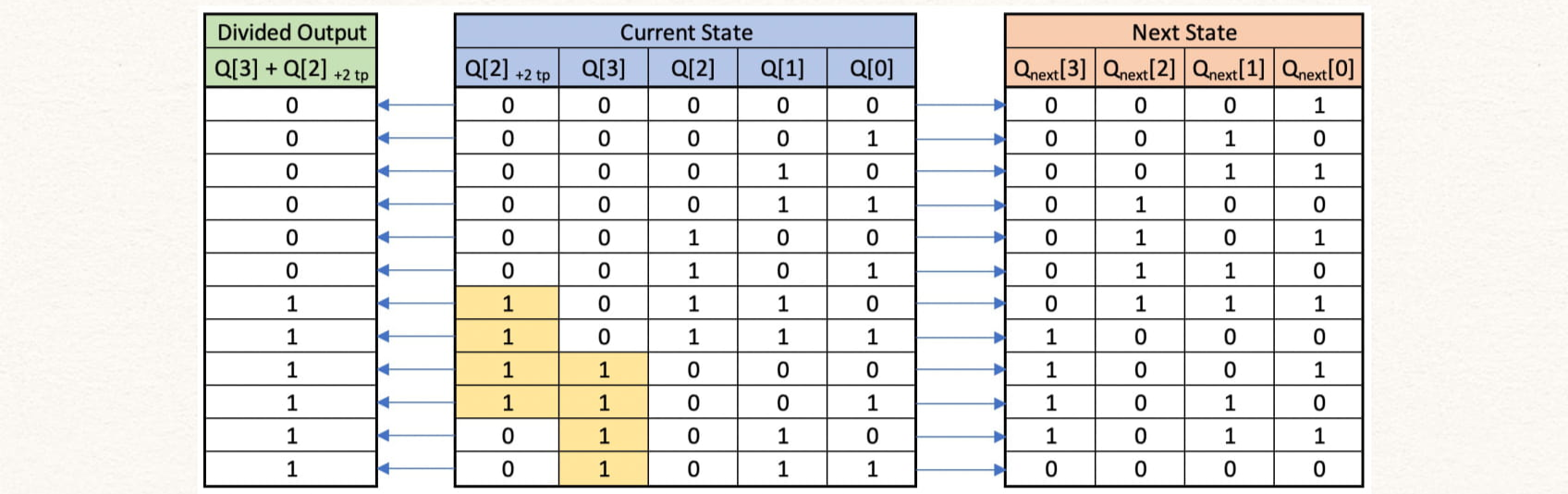
The table shows the current counter state and the next state. The first column shows the clock divider output.

Here, tp stands for time period of the clock, i.e. + 2 tp stands for the signal delayed by 2 clock periods.
The same can be modelled in verilog as:
module div_by_12 (input clk, rst,
                 output clk_out);

  // Registers to store the current count value and wire to compute the next count value
  reg [3:0] Q, Q_next;

  // Registers to delay Q[2] signal by 2 clock period
  reg Q_delay_1tp, Q_delay_2tp;


  // Combinational logic to compute the next state logic (count value)
  always @ (*) begin
    if (Q == 4'd11)
      Q_next = 4'h0;	// If counted to 11, set Q to 0
    else
      Q_next = Q + 1; 	// If not counted to 11, set Q to Q + 1
  end

  // State memory
  always @ (posedge clk) begin
    if (rst)
      Q <= 4'h0;	// If reset, set Q to 0
    else
      Q <= Q_next;	// If not reset, set Q to the next count value
  end

  // Always block to delay Q[2] by 2 clock cycle
  always @ (posedge clk) begin
    if (rst) begin
      Q_delay_1tp <= 1'b0;
      Q_delay_2tp <= 1'b0;
    end
    else begin
      Q_delay_1tp <= Q[2];
      Q_delay_2tp <= Q_delay_1tp;
    end
  end

  // The clk/12 is set when Q[2]_delayed_by_2_cycle == 1 or Q[3] == 1
  assign clk_out = Q_delay_2tp | Q[3];

endmodule
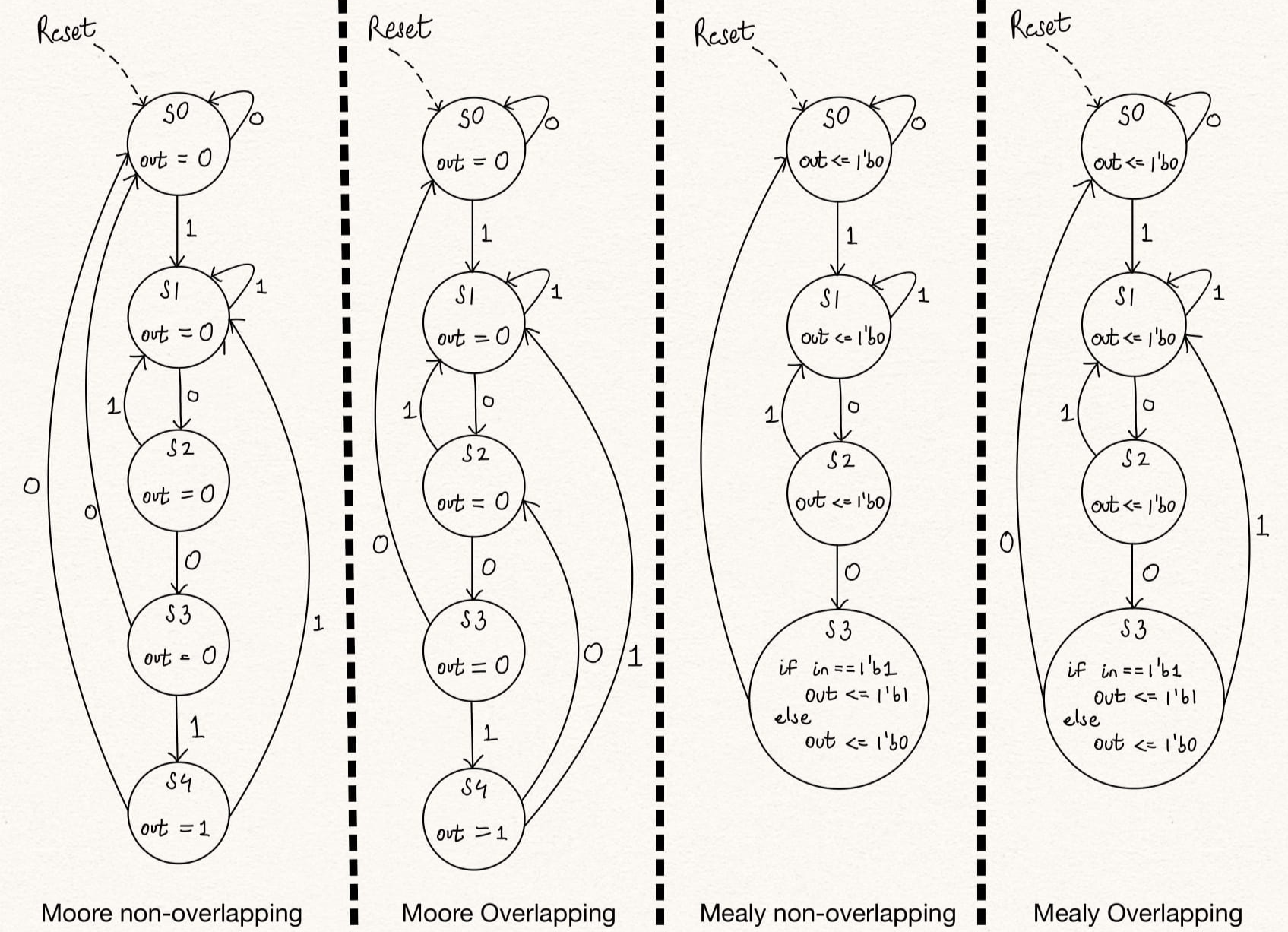
A simple sequence detector can be modelled in several ways -
1. Non-overlapping - Here, consider a sequence detector for sequence 1010. For the input sequence 10101010 the output will be 00010001, i.e. the sequence is detected in a non-overlapping fashion. Once a sequence is detected, the sequence needs to be repeated completely from the start to be dected again.
2. Overlapping - Again, consider a sequence detector for sequence 1010. For the input sequence 10101010 the output will be 00010101, i.e. the sequence is detected in an overlapping fashion. Once a sequence is detected, a new sequence can be detected using a part of the previously detected sequence when applicable.
Also, the state machine being used to detect the sequence can be mealy or a moore state machine. This will change the total number of states at some cost to the output functional logic
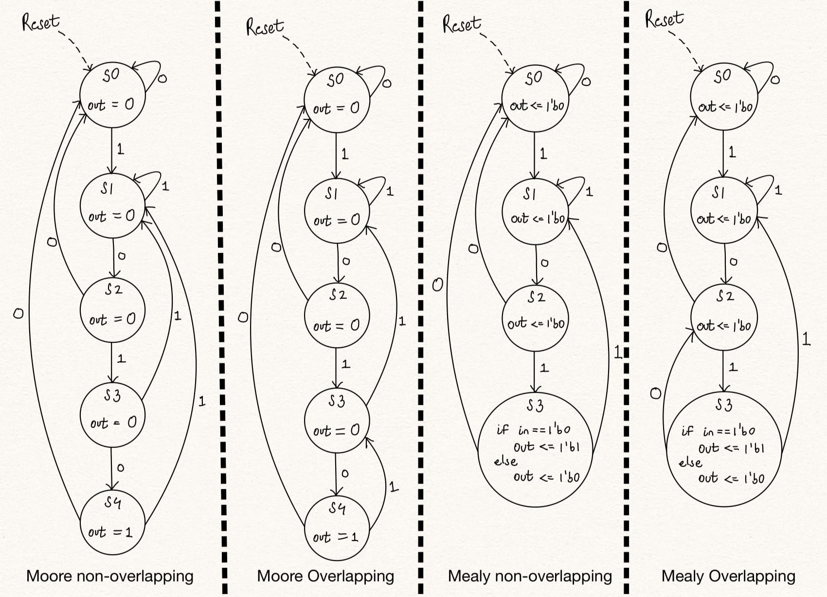
Figure: Sequence Detector 1010 - Moore and Mealy; non-overlapping and overlapping state machines.
// Code your design here
module seq_1010(input din, clk, rst,
                output dout);

  // Parameterized state values for ease
  parameter S0 = 0, S1 = 1, S2 = 2, S3 = 3, S4 = 4;

  // RState memory definition
  reg [2:0] state, next_state;

  // Next State Logic - combinational logic to compute the next state based on the current state and input value
  always @ (*) begin
    case (state)
      S0: next_state = din ? S1 : S0;
      S1: next_state = din ? S1 : S2;
      S2: next_state = din ? S3 : S0;
      S3: next_state = din ? S1 : S4;
      S4: next_state = din ? S1 : S0; // This transition for non-overlaping sequence detector (If uncommented, comment the next line)
      //S4: next_state = din ? S3 : S0; // This transition for overlaping sequence detector (If uncommented, comment the previous line)
      default: next_state = S0;
    endcase
  end

  // State Memory - Assign the computed next state to the state memory on the clock edge
  always @ (posedge clk) begin
    if (rst) state <= 3'b000;
    else state <= next_state;
  end

  // Output functional logic - The states for which the output should be '1'
  assign dout = state == S4;
endmodule
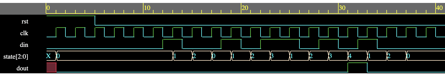
Figure: Sequence Detector 1010 - Moore non-overlapping waveform.
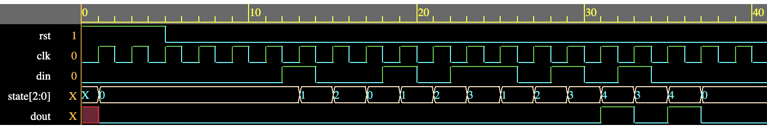
Figure: Sequence Detector 1010 - Moore overlapping waveform.
// Code your design here
module seq_1010(input din, clk, rst,
                output reg dout);

  // Parameterized state values for ease
  parameter S0 = 0, S1 = 1, S2 = 2, S3 = 3;

  // RState memory definition
  reg [1:0] state, next_state;

  // Next State Logic - combinational logic to compute the next state based on the current state and input value
  always @ (*) begin
    case (state)
      S0: next_state = din ? S1 : S0;
      S1: next_state = din ? S1 : S2;
      S2: next_state = din ? S3 : S0;
      S3: next_state = din ? S1 : S0;// This transition for non-overlaping sequence detector (If uncommented, comment the next line)
      //S3: next_state = din ? S1 : S2; // This transition for overlaping sequence detector (If uncommented, comment the previous line)
      default: next_state = S0;
    endcase
  end

  // State Memory - Assign the computed next state to the state memory on the clock edge
  always @ (posedge clk) begin
    if (rst) state <= 2'b00;
    else state <= next_state;
  end

  // Output functional logic - The states for which the output should be '1'
  always @ (posedge clk) begin
    if (rst) dout <= 1'b0;
    else begin
      if (~din & (state == S3)) dout <= 1'b1;
      else dout <= 1'b0;
    end
  end
endmodule
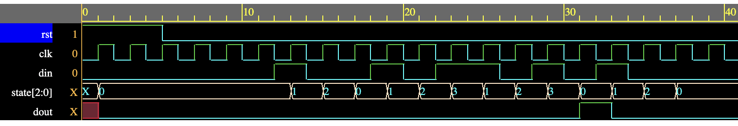
Figure: Sequence Detector 1010 - Mealy non-overlapping waveform.
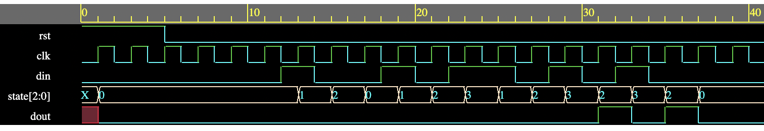
Figure: Sequence Detector 1010 - Mealy overlapping waveform.
The sequence can also be detected using a simple n-bit shift register, where "n" represents the length of the sequence to be detected (in this case 4) and a comparator can be used to check the state of these n-bit registers. However, consider a sequence which has 20 bits, then we will need a 20 bit shift register which happens to be extremely costly in terms of area. The same can be acheived using a state machine with just 5 flip-flops and some additional combinational logic.
module seq_1001_moore (input din, clk, rst,
                output dout);

  // Parameterized state values for ease
  parameter S0 = 0, S1 = 1, S2 = 2, S3 = 3, S4 = 4;

  // RState memory definition
  reg [2:0] state, next_state;

  // Next State Logic - combinational logic to compute the next state based on the current state and input value
  always @ (*) begin
    case (state)
      S0: next_state = din ? S1 : S0;
      S1: next_state = din ? S1 : S2;
      S2: next_state = din ? S1 : S3;
      S3: next_state = din ? S4 : S0;
      S4: next_state = din ? S1 : S0; // This transition for non-overlaping sequence detector (If uncommented, comment the next line)
      //S4: next_state = din ? S1 : S2; // This transition for overlaping sequence detector (If uncommented, comment the previous line)
      default: next_state = S0;
    endcase
  end

  // State Memory - Assign the computed next state to the state memory on the clock edge
  always @ (posedge clk) begin
    if (rst) state <= 3'b000;
    else state <= next_state;
  end

  // Output functional logic - The states for which the output should be '1'
  assign dout = state == S4;
endmodule
Figure: Sequence Detector 1001 - Mealy non-overlapping waveform.
Figure: Sequence Detector 1001 - Mealy overlapping waveform.
module seq_1001_mealy (input din, clk, rst,
                output reg dout);

  // Parameterized state values for ease
  parameter S0 = 0, S1 = 1, S2 = 2, S3 = 3;

  // RState memory definition
  reg [2:0] state, next_state;

  // Next State Logic - combinational logic to compute the next state based on the current state and input value
  always @ (*) begin
    case (state)
      S0: next_state = din ? S1 : S0;
      S1: next_state = din ? S1 : S2;
      S2: next_state = din ? S1 : S3;
      S3: next_state = S0;// This transition for non-overlaping sequence detector (If uncommented, comment the next line)
      //S3: next_state = din ? S1 : S0; // This transition for overlaping sequence detector (If uncommented, comment the previous line)
      default: next_state = S0;
    endcase
  end

  // State Memory - Assign the computed next state to the state memory on the clock edge
  always @ (posedge clk) begin
    if (rst) state <= 2'b00;
    else state <= next_state;
  end

  // Output functional logic - The states for which the output should be '1'
  always @ (posedge clk) begin
    if (rst) dout <= 1'b0;
    else begin
      if (din & (state == S3)) dout <= 1'b1;
      else dout <= 1'b0;
    end
  end
endmodule
Figure: Sequence Detector 1001 - Mealy non-overlapping waveform.
Figure: Sequence Detector 1001 - Mealy overlapping waveform.
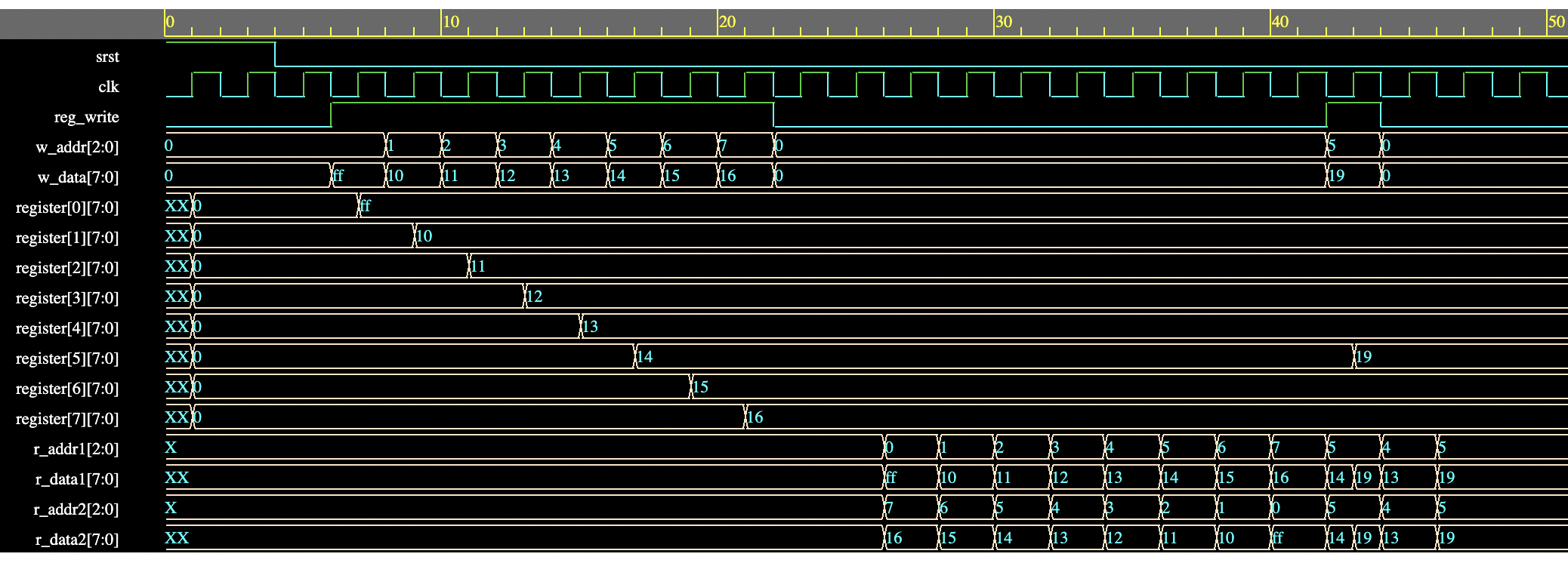
Register File is a type of memory block (typically used in a CPU), a m-set of storage cells to store data n-bit wide. It is used to hold data and fetch data based on the need. To perform this function, the register has the write operation to enable writing data to the register locations and read operation to enable reading the register locations. To write and read data the register file has write pointer and read pointer inputs which can be in a binary encoded or one-hot coded fashion. The number of writes and reads that can be performed in a clock cycle decide the number of write port and read ports needed in a register file.
The most common use of a register file is in a CPU in which we can perform a write to store the computed data and 2 reads to fetch data operands to operate on in a clock cycle. For this reason, we will design a register file with 1 write port and 2 read ports.
At the transistor level, register file can be an array of flip flops. However, in larger designs this is costlier and it is implemented through SRAM cells. However, with an SRAM cell array there is additional considerations of read and write cycles.
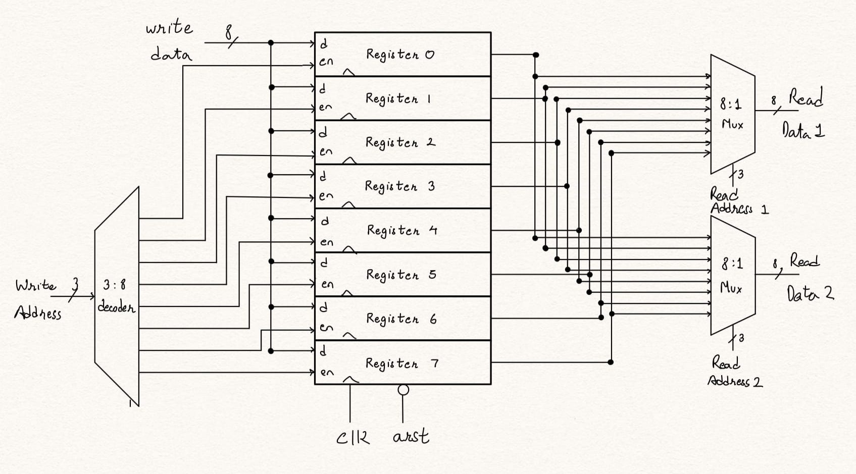
Figure: Register file with 1 write port and 2 read ports
Register file operations include:
- Register File Read Operation: A read address value is provided on the read address port to select the register to be read from. The read data is available immediately through the mux coming out on the read data port.
- Register File Write Operation: A write address value is provided on the write address port to select the register to which data is to be written and write data value is provided on the write data port which is the data to be written to.
module RegisterFile ( input clk, srst, reg_write,
                     input [7:0] w_data,
                     input [2:0] r_addr1, r_addr2, w_addr,
                     output [7:0] r_data1, r_data2);

  // Register memory array - 8 locations of 8 bits each
  reg [7:0] register [0:7];

  integer i;

  always @ (posedge clk) begin
    if (srst) begin

      // Initialize all registers to value 0
      for(i = 0; i < 8; i=i+1) begin
        register[i] <= 'h0;
      end
    end
    else if (reg_write)

      // Write to registers only on condition reg_write
      // On reg_write, write the data to the register address provided on w_addr
      register[w_addr] <= w_data;
    end

  // Read data available on 2 read ports based on 2 seperate read addresses
  assign r_data1 = register[r_addr1];
  assign r_data2 = register[r_addr2];

endmodule
In this day, almost every digital component works on a clock and it is very common that the sub-systems exchange data for computational and operational needs. An intermediary becomes necessary if:
- The data produced and the data consumer operate on different clock frequencies
- If the data is being produced at a slower speed than the data is being consumed (f_write_clk < f_read_clk) the data transfer can take place through a single data register followed by asynchronous data synchronization methods (handshake or 2-clock synchronization)
- If the data is being produced at a higher speed than the data is being consumed (f_write_clk > f_read_clk) the data transfer needs buffering which can be implemented through an asynchronous FIFO. The depth of the FIFO depends the write and read clock and the maximum data burst length.
- The data producer and the data consumer have a skew between their clocks
- If the data is being produced at the same speed as the data is being consumed (f_write_clk = f_read_clk) and there is a skew between the producer and the consumer clock, the data can be transferred through a lock-up latch/register to overcome the skew
- There is a skew between the data production burst and data reception burst
- If the producer and consumer operate at the same clock but have a large skew between when a burst of data is produced and when the burst of data is consumed. In such scenario, the produced data needs to be buffered and the sequence of transfer needs to be preserved, then a synchronous FIFO can be used. The depth of such FIFO is decided by the maximum burst length
Additional information can be found at FIFO Architecture, Functions, and Applications
Additional info on deciding the fifo depth can be found at Calculation of FIFO Depth
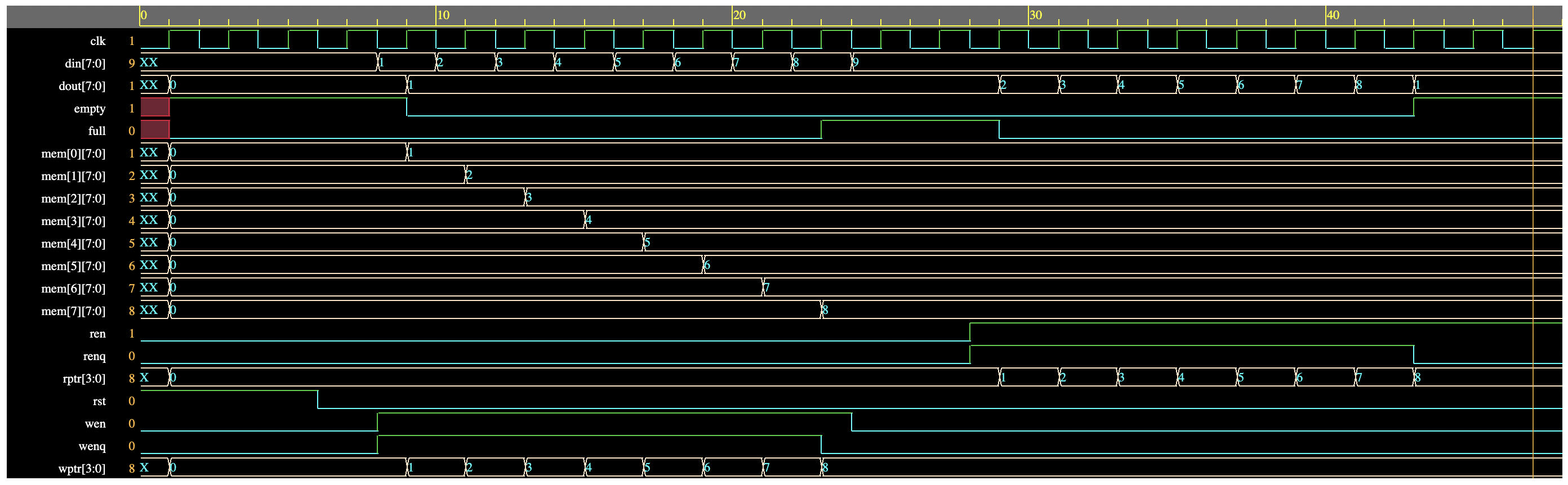
Synchronous FIFO - The type of FIFOs which have common write and read clock are called synchronous FIFO. Synchronous FIFOs are very common in a processor/controller ICs which work on a common system clock. Since all the sub-systems work on the same system clock they can make use of sync-FIFOs with a possible need for skew handling.
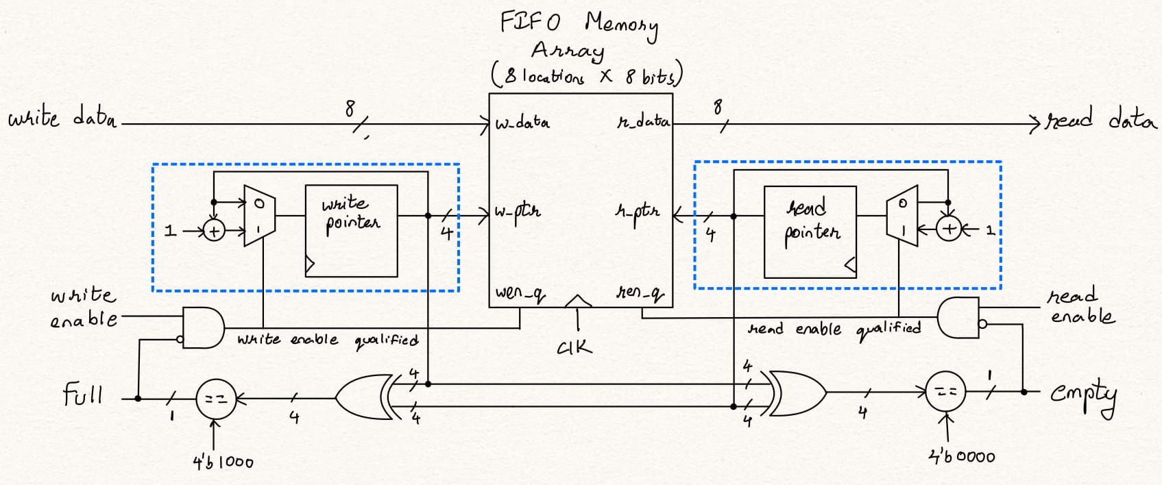
module fifo(input clk, rst, wen, ren,
            input [7:0] din,
            output full, empty,
            output reg [7:0] dout);

  // FIFO memory array - 8 locations of 8 bits each
  reg [7:0] mem [0:7];

  // FIFO write and read pointer registers (n+1) bit wide
  reg [3:0] wptr, rptr;

  // read enable and write enable qualified signals declaration
  wire wenq, renq;

  // Computation of full and empty signals based on the current
  // read and qrite pointers
  assign full = ((wptr ^ rptr) == 4'b1000);
  assign empty = (wptr == rptr);

  // read enable qualified and write enable qualified are generated
  // based on the write/read request and full and empty status of FIFO
  assign wenq = ~full & wen;
  assign renq = ~empty & ren;

  always @ (posedge clk) begin

    if (rst) begin
      // Write and read pointers are initialized to 0
      wptr <= 4'b0000;
      rptr <= 4'b0000;

      // FIFO memory is initialized to 0 (not necessary)
      for (integer i = 0; i < 8; i = i + 1)
        mem[i] = 8'h00;
    end
    else begin
      // Write pointer is incremented on valid write request
      // FIFO memory is updated with data for valid write request
      if (wenq) begin
        wptr <= wptr + 1;
        mem[wptr] <= din;
      end
      else begin
        wptr <= wptr;
        mem[wptr] <= mem[wptr[2:0]];
      end

      // Read pointer is incremented on valid read request
      if (renq)
        rptr <= rptr + 1;
      else
        rptr <= rptr;
    end
  end

  // Read data port
  assign dout = mem[rptr[2:0]];

endmodule
Typically, a FIFO has 2^n locations and for such a FIFO a n+1 bit write and read pointers are used. However, in a FIFO with odd depth, i.e., which has locations not equal to 2^n we will continue to use a n+1 bit write and read pointers but these will be implemented as a mod-n counter.
For example, say we need to design a FIFO with 6 locations we need 4-bit read and write pointers of which the lower three bits will sequence from 3'b000, 3'b001, 3'b010, 3'b011, 3'b100, 3'b101 to point to the FIFO memory locations.
The same can be modelled in verilog as,
module FIFO(input clk, wen, ren, rst,
            input [7:0] data_in,
            output full, empty,
            output [7:0] data_out);

  // FIFO write and read pointer registers (n+1) bit wide
  reg [3:0] wptr, rptr;

  // FIFO memory array - 8 locations of 8 bits each
  reg [7:0] mem [0:5];

  // Computation of full and empty signals based on the current
  // read and qrite pointers
  assign full = (wptr ^ rptr) == 4'h8;
  assign empty = wptr == rptr;

  // read enable qualified and write enable qualified are generated
  // based on the write/read request and full and empty status of FIFO
  assign wenq = ~full & wen;
  assign renq = ~empty & ren;

  always @ (posedge clk) begin
    if (rst) begin
      // FIFO memory is initialized to 0 (not necessary)
      for (integer i = 0; i < 8; i=i+1)
        mem[i] <= 8'h00;

      // Write and read pointers are initialized to 0
      wptr <= 4'h0;
      rptr <= 4'h0;
    end
    else begin
      // Write pointer is incremented on valid write request
      // FIFO memory is updated with data for valid write request
      if (wenq) begin
        if (wptr[2:0] == 3'b101)
          wptr <= {~wptr[3], 3'b000};
        else
          wptr <= wptr+1;
        mem[wptr[2:0]] <= datain;
      end

      // Read pointer is incremented on valid read request
      if (renq) begin
        if (rptr[2:0] == 3'b101)
          rptr <= {~rptr[3], 3'b000};
        else
          rptr <= rptr+1;
      end
    end
  end

  // Read data port
  assign dataout = mem[rptr[2:0]];

endmodule
Asynchronous FIFO - The type of FIFOs which have different write and read clock are called asynchronous FIFO. Such FIFO block is typically used when data needs to be transferred across clock-domain-crossing (CDC), where both the producer and the consumer work in different clock domain.
Click here to visit website with extensive documentation of verilog
Click here to visit an exceptional compilation of basic verilog for ASIC design
Website Version: 1.08.054