This design is GDSII ready (although there are a few MAX_FANOUT violations to
sort out) using the SkyWater 130nm
PDK and the
OpenLane RTL-to-GDSII flow
that is part of the OpenROAD
project.
To run the flow yourself,
- Set up the environment as shown in the OpenLane documentation.
- Use the provided
config.tcl. - Copy the contents of the
hdl/directory to thesrc/directory in your OpenLane design environment.
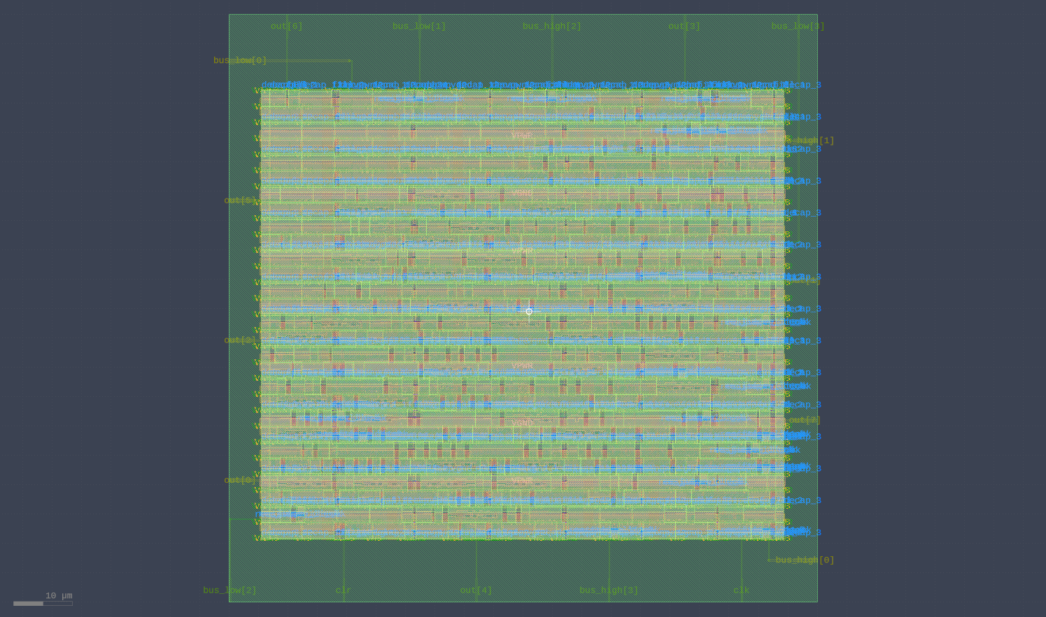 |
|---|
| Klayout GDSII view |
| ✨ Thanks to GDS2WebGL, you can view and explore GDSII layouts in the browser (even on mobile)!! ✨ Check it out! |
Edit the contents of
hdl/rom16_8bit.v
to change the program as this computer is programmed directly in ROM.
 |
|---|
| Waveform output for default program |
The following structure is followed:
    .
    ├── hdl
    ├── test
    └── img
- All Verilog modules are located in the
hdldirectory- Only ONE Verilog module exists per
.vfile
- Only ONE Verilog module exists per
- All Verilog test-benches are located in the
testdirectory- Filenames for testbenches are prefixed with
tb- E.g.
dff_posedge.v -> tb_dff_posedge.v
- E.g.
- Output files (
*.out) after compilation are also located in thetestdirectory
- Filenames for testbenches are prefixed with
- Waveform dumps are put in the
simulationdirectory (create it if it doesn't exist). - Any images used are placed in the
imgdirectory
iverilogis used to compile and test the code. To view waveforms, use a program likegtkwave.
There are two helper scripts to simplify this step.
To compile, use the compile.sh script. Usage is as follows:
# To compile all files in the test directory
$ ./compile.sh

# To compile specific files
$ ./compile.sh FILE1 FILE2 ...
To run compiled files, use the run.sh script.
Usage is as follows:
# To run all compiled files in the test/ directory
$ ./run.sh

# To run compiled files
$ ./run.sh FILE1 FILE2 ...
To open waveform dump (gtkwave is used here): gtkwave <path-to-vcd-file>
-
The SAP (Simple-As-Possible)-1 Computer is an 8-bit computer capable of performing simple operations such as add and subtract two numbers.
-
The SAP-1 employs a processing unit (ALU + Registers), a control unit, memory to store data and instructions and a central bus.
-
It is a stored-program computer in which fetch and execute cycles occur separately as they share a common bus.
-
It is built using the bottom-up approach where all the sub-modules are constructed initially and finally assembled to deploy a working computer.
The figure below represents the architecture of SAP-1 computer.
 |
|---|
| SAP-1 Architecture |
The architecture of SAP-1 has the following components:
- Program Counter
- Memory Address Register
- Memory
- Instruction Register
- Controller-Sequencer
- Accumulator
- Adder-Subtractor
- B-Register
- Output Register
"When software talks to hardware, it has a vocabulary. The words are called instructions, and the vocabulary is called the Instruction Set Architecture (ISA)"
-- David Patterson

| Mnemonic | Operation | Op-code |
|---|---|---|
| LDA | Load RAM data into Accumulator | 0000 |
| ADD | Add RAM data into Accumulator | 0001 |
| SUB | Subtract RAM data from Accumulator | 0010 |
| OUT | Load Accumulator data into Output Register | 1110 |
| HLT | Stop processing | 1111 |
Every instruction and required data has to be fetched from the memory.
Correspondingly, the processor executes the instruction and outputs the result using the output register.
This process happens in two cycles, i.e. Fetch & Execute across six different timing states accounted by a 6-bit ring-counter.
 |
|---|
| "T-states" (timing states) |
The controller-sequencer outputs 12 different control signals which are key to the computer's automatic operation.
Every signal supervises and tells the computer about what needs to be done at what stage.
All the signals are listed below:
inc= INCREMENTpc_out_en= OUTPUT ENABLE OF PROGRAM COUNTERlow_ld_mar= LOAD MARlow_mem_out_en= CHIP ENABLE FOR RAMlow_ld_ir= LOAD INSTRUCTION REGISTERlow_ir_out_en= OUTPUT ENABLE OF INSTRUCTION REGISTERlow_ld_acc= LOAD ACCUMULATORacc_out_en= OUTPUT ENABLE OF ACCUMULATORsub_add= SUBTRACTION/ADDITIONsubadd_out_en= OUTPUT ENABLE OF SUBTRACTION/ADDITIONlow_ld_b_reg= LOAD B REGISTERlow_ld_out_req= LOAD OUTPUT REGISTERlow_halt= HALT EXECUTION
Inspired by Ben Eater's 8-bit Computer
- YouTube Playlist on SAP-1
- Simulation of SAP-1
- Digital Computer Electronics by Albert Paul Malvino & Jerald A. Brown
- Advanced Digital Design with the Verilog HDL by Michael D. Ciletti
- Verilog HDL: A Guide To Digital Design & Synthesis by Samir Palnitkar
- OpenROAD website
- OpenLane documentation
- Google SkyWater PDK documentation
- Fork this repo, and create a new branch for the feature you are developing
- Take a look at the TODO
- Keep the directory structure as it is.
- Enable editorconfig for your editor to take care of formatting
- Keep commit messages concise and meaningful
This project is licensed using the GPL-v3 license