Solar Panel Board
Schematic:

Note The Raspberry Pi has 3 I2C buses, and I am using two of them, /dev/i2c-1 and /dev/i2c-0. On /dev/i2c-1, J7, J8, J9, and J10 are addresses 0x40, 0x41, 0x44, and 0x45. These are a minimal set of sensors on the X+, Y+, and Z+ solar panels and the NiMH battery. The Digital Transceiver board uses address 0x48 on this bus as a temperature sensor which is used in the telemetry. If a X- and Y- solar panel is present, then J11 and J12 are used on the /dev/ic2-0 bus with addresses 0x40 and 0x41. The addresses are set on the INA219 boards by solder jumpers - see the Addressing the Boards section of https://learn.adafruit.com/adafruit-ina219-current-sensor-breakout/assembly. I don't know why the addressing skips 0x42 and 0x43.
Building Information:
KiCad files https://github.com/alanbjohnston/CubeSatSim/tree/master/kicad
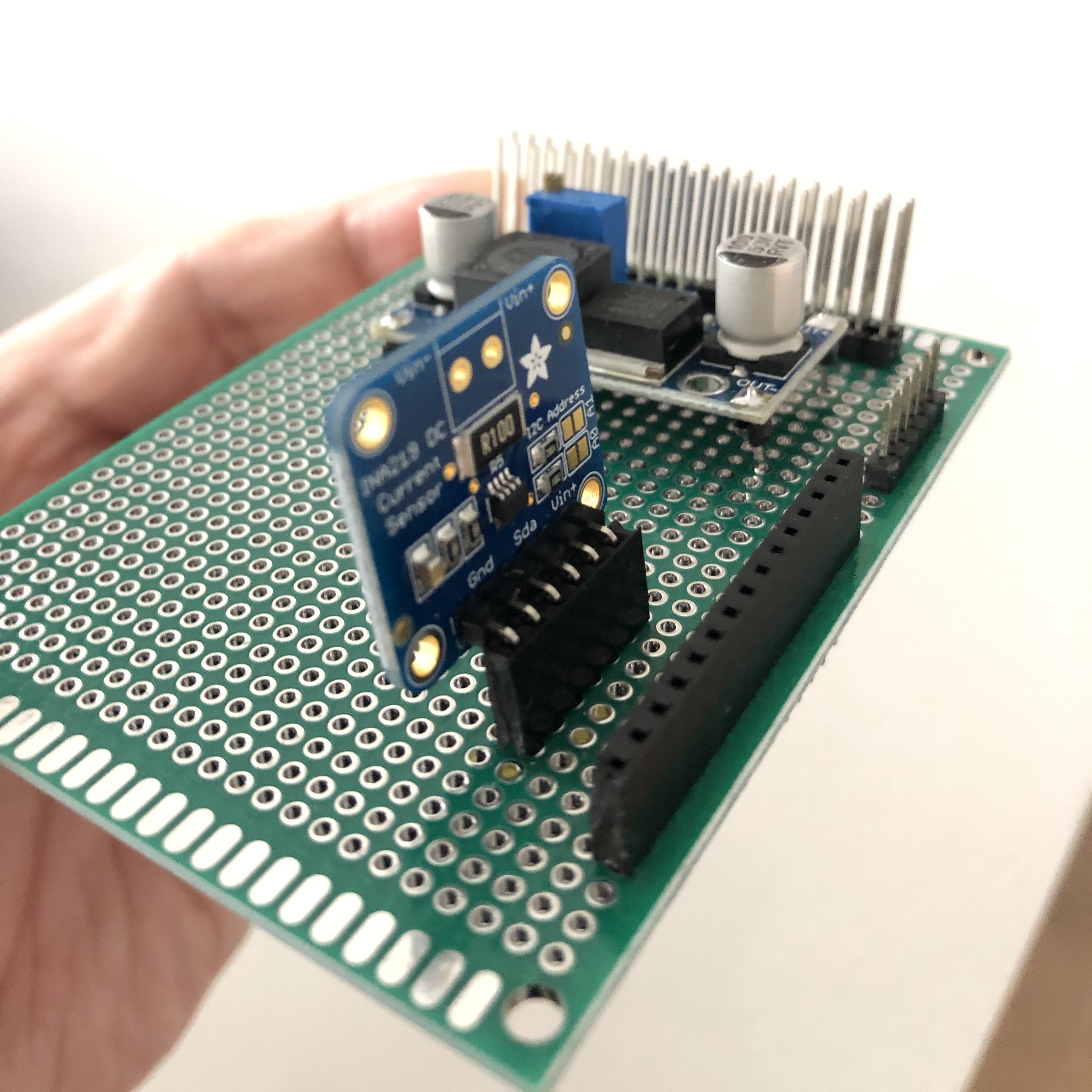
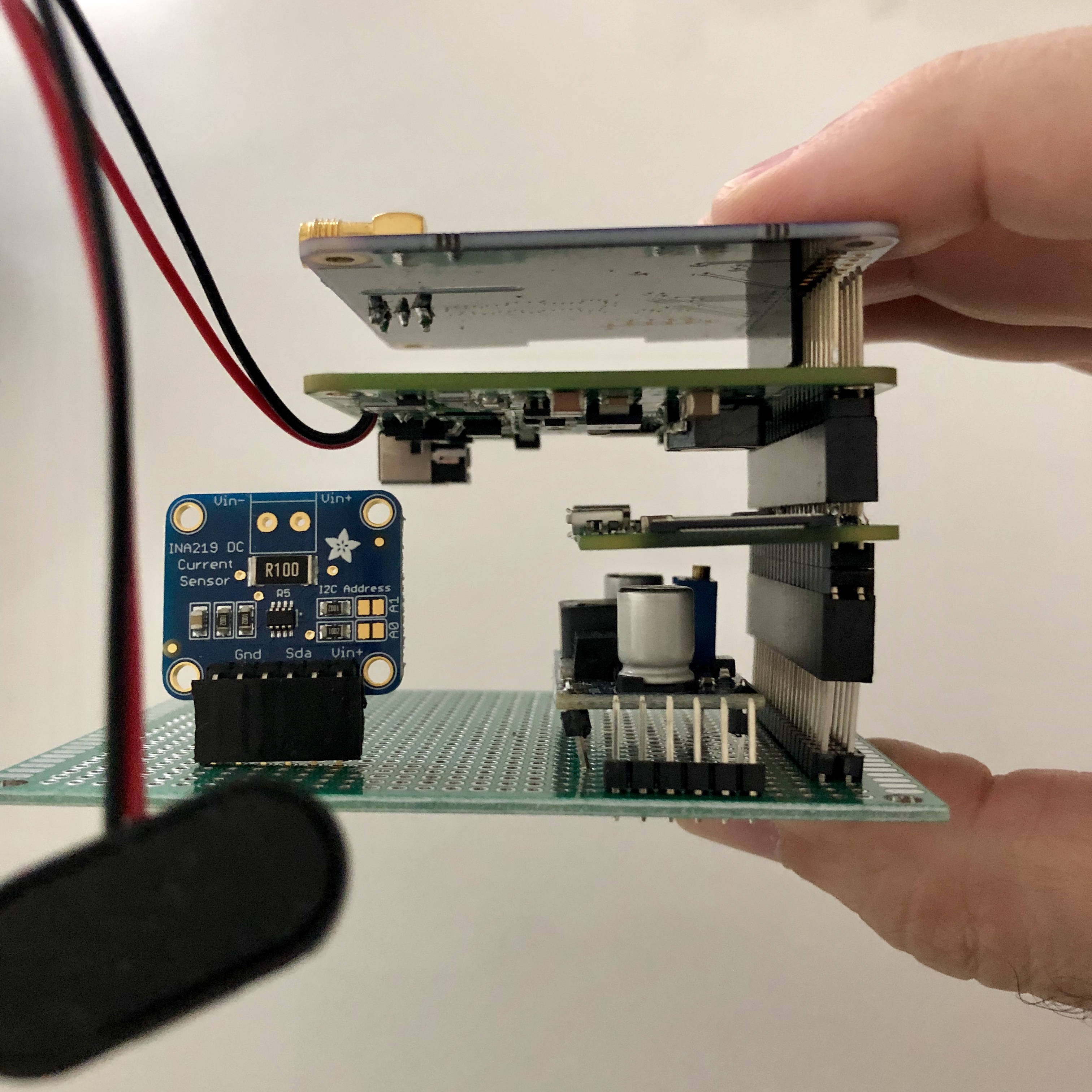
Here are some mockups of the PCB layout showing how I plan to mount the INA219 boards vertically
Here is a preliminary (untested) PCB board design:

Assembly of PCB Instructions:
Materials:
- 1x AMSAT CubeSat Simulator Solar Power Board PCB
- 1x 40 pin extra long (19mm) male breakaway headers, straight
- 1x 40 pin regular length male breakaway headers, straight
- 2x 40 pin regular length female headers
- 1x Boost module
- 5x diodes, 1N5817
- 2x resistors 4.7k Ohm, 1/4 watt
- 6x INA219 Sensor boards
- 1x 40 pin right angle male breakaway headers
Steps:
-
Break 40 pin extra long male breakaway header into two 20 pin headers, and use for GPIO connector. Solder into place, being careful that the two rows are parallel and at right angle to the board (A 2x20 pin stackable header could be inserted into them a short way to ensure this). After it cools, test plugging into Pi Zero W board stackable header. Note: not every pin needs to be soldered: required pins:1,2,3,4,5,6,9,14,20,25,27,28,30,34,39.
-
Break 40 pin regular length male breakaway header into 2x 2 pin (J3, J4) and 1x 5 pin (J5). Solder J3, J4, and J5 into board.
-
Solder resistors R1 and R2 vertically.
-
Break off 4 single pins from the regular length male breakaway header and solder into the four terminals of the Boost Converter Module for IN+, IN-, OUT+, and OUT-. When cool, test fit the module into the PCB - reheat pins if necessary to fit. Solder in Boost Converter Module into U1.
-
Solder diodes D1, D2, D3, D4, and D5 vertically. Cathode (marked by a band on diode package) goes into the round hole (on right), while the Anode goes into the square hole (on left). CHECK: Seems to be reversed!
-
Cut two 40 pin female headers into 1x 5 pin (J6), 6x 6 pin (J7, J8, J9, J10, J11, J12), 1x 12 pin (A combined J1 and J2 connector). See https://www.instructables.com/id/How-to-cut-pin-headers/ for good tips on how to sacrifice one pin to ensure the cut header has full stregth.
-
Cut 90 degree breakaway headers into 6x 6 pin lengths.
-
Set the correct I2C bus address on the 6x INA219 boards by adding solder to jumpers to bridge A0 and A1 as needed. See instructions at https://learn.adafruit.com/adafruit-ina219-current-sensor-breakout/assembly (Note: do not use the pins and connectors that came with the INA219 board). Set the jumpers using this list:
- J7 X+ Board: Bus /dev/i2c-1 Address = 0x40 Offset = binary 00000 (no jumpers required)
- J8 Y+ Board: Bus /dev/i2c-1 Address = 0x41 Offset = binary 00001 (bridge A0)
- J9 Z+ Board: Bus /dev/i2c-1 Address = 0x44 Offset = binary 00100 (bridge A1)
- J10 Vbatt Board: Bus /dev/i2c-1 Address = 0x45 Offset = binary 00101 (bridge A0 and A1)
- J11 X- Board: Bus /dev/i2c-0 Address = 0x40 Offset = binary 00000 (no jumpers required)
- J12 Y- Board: Bus /dev/i2c-0 Address = 0x41 Offset = binary 00001 (bridge A0)
-
Solder the 6 pin 90 degree headers into the boards so the pins face downward.
-
Test fit the INA219 boards vertically into connectors J7 through J12, but do not leave them plugged in.
Remove Before Flight (RBF) Switch
Materials:
- 1x 3.5mm TRS female audio jack with 2 switches
- 1x 3.5mm TRS male plug
- 6x female jumper wires (keep attached together if possible)
Steps:
- Plug female ends of jumper wires into J5 connector and measure length for position of RBF switch. Cut to length and trim wires
- Solder onto 3.5mm audio jack per schematic
- Remove screw cover on male TRS plug and drill hole through for mounting RBF tag or other handle
- Cut jumper wire short enough to stay inside the cover to connect pins 3 and 1 (center and outer conductors). Solder jumper wire and put cover back on
- Attach RBF tag, taking care not to hit the jumper or connector.
- Test switch while unplugged from PCB with DMM set to Ohms or continuity:
- With the plug in, there is a short circuit between pins 4 and 5. There is an open circuit between pins 1 and 2, and pins 3 and 4.
- With the plug out, there is a short circuit between pins 1 and 2, and between pins 1 and 2, and pins 3 and 4. There is an open circuit between pins 3 and 4.
- Plug into J5 of PCB and mount switch on CubeSat frame on top.
DC Charging Cable
Materials
- 1x Barrel power connector 5.5mm x 2.1mm female
- 2x Female jumper wires
Steps:
- Plug female jumper wires into connector J2. Measure and cut length based on barrel connector mount position on frame
- Solder wires to connector.
- Connect center of barrel connector to J2 pin 1. Connect center of barrel connector to J2 pin 2.
Battery Monitoring Cable
Materials:
- 2x 9V snap connector wires
- 1x Male breakaway header strip
Steps:
- Break off a 1x2 male header.
- Solder the positive lead (red wire) of one connector to one pin of the 1x2 male header, and solder the negative lead (black wire) of the other connector to the other pin of the 1x2 male header.
- Solder the other ends of the two connectors together.
- Plug into J2 with the positive lead of the connector plugged into pin 1, and the negative lead of the connector plugged into pin 2.
- Plug the NiMH battery into the connector that the positive lead is wired to the header connector. Plug the connector from the MoPower UPS V2 board into the other connector. CHECK!
Putting it all together and Testing
-
Plug Pi Zero W board into this board. Power up Pi and make sure Pi works fine. Check J6 for 3.3V (pin 2 to pin 3) and 5V supply (pin 2 to pin 3). Check for 3.3V for pin 6 to 5 of J7 - J11. Shutdown the Pi.
-
Plug in INA219 boards to J7 - J11 and power up the Pi. Run i2cdetect 1 command on Pi. You should see each INA219 Board you have plugged in (40, 41, and 44, and 45 for J7, J8, J9, and J10) (If you have the Digital Transceiver Board plugged into the Pi, you will see 4a as well). If not, check A0 and A1 jumpers and soldering of the missing board. Run i2cdetect 0 command on Pi. You should see each INA219 Board you have plugged in (40 and 41 for J11 and J12). If not, check A0 and A1 jumpers and soldering of the missing board.
-
Run the Sensor only software on the Pi. You should see results for all the boards. Plug in an illuminated solar panel into J1 for X+ (pin 1 to + and pin 2 to -) and rerun the Sensor only software - you should see the X+ voltage, and zero current and zero power. Repeat for Y+, Z+, X-, and Y- (if you have them) (pins 3 and 4, pins 5 and 6, pins 7 and 8, and pins 9 and 10).
-
Shutdown the Pi. Plug the 2 pin male connector on the battery monitoring cable into J2. Run the Sensor only software and you should read the battery voltage and the current and power (if the Pi is powered up).
-
With one or more illuminated solar panels plugged into J1, you should read a voltage on J5, pin 1, of around your open circuit solar panel voltage - 0.5V. With the RBF pin out, plug in the RBF switch connector to J5. You should measure a voltage on J4 pins 1 to 2 - this is the output of the boost converter module. Shutdown the Pi and unplug it from the GPIO connector.
-
With the Pi not plugged in, you can adjust the trimpot on the boost converter U1 so that the voltage on J4 pins 1 to 2 reads around 15V. It may take a few turns. Put the RBF pin back in, and the voltage on J4 pins 1 to 2 should drop to zero.
-
With the RBF pin plugged in, plug in the DC in barrel power cable into J3. With a power pack plugged into AC, you should read around 15V on J4 pin 1 to 2.
-
On the MoPower UPS V2 board, solder two 90 degree male headers into the Vin2 + and - holes. Mount the headers on the top of the PCB (same side as the chips and components) and angle them towards the GPIO connector. If a DC power pack is plugged into the MoPower board, unplug it. Use a red and black pair of female to female jumper wires to connect the Vin2+ to J4 pin 1, and Vin2 - to J4 pin 2. With the RBF pin inserted and the Pi powered up, plug the power pack into the barrel connector on the PCB and verify using the Sensor only software that the battery pack is charging.
-
With the RBF pin removed and the solar panels covered or unplugged, note the current and power supplied by the battery. Illuminate one or more solar panels and verify using the Sensor only software that the battery current and power is lower.
-
On the Pi, run the ./radioafsk application and note the telemetry. Vary the illumination level and position, and you should see that reflected in the telemetry.
-
Place the Sim on the turntable in front of the halogen lamp and switch on to lowest rotation rate. Capture the telemetry and analyze using the spreadsheet. You should be able to calculate the rotation rate of the Sim based on the period of the solar panel current waveforms.