-
Notifications
You must be signed in to change notification settings - Fork 91
Pico and Solar SMD
These are the instructions for building the Pico Board and Solar Board as full Surface Mount Device (SMD) Boards
Here is the software for the CubeSatSim Pico: https://github.com/alanbjohnston/CubeSatSim/tree/pico/cubesatsim
These are the instructions for building the Pico v0.5s board SMD Components.
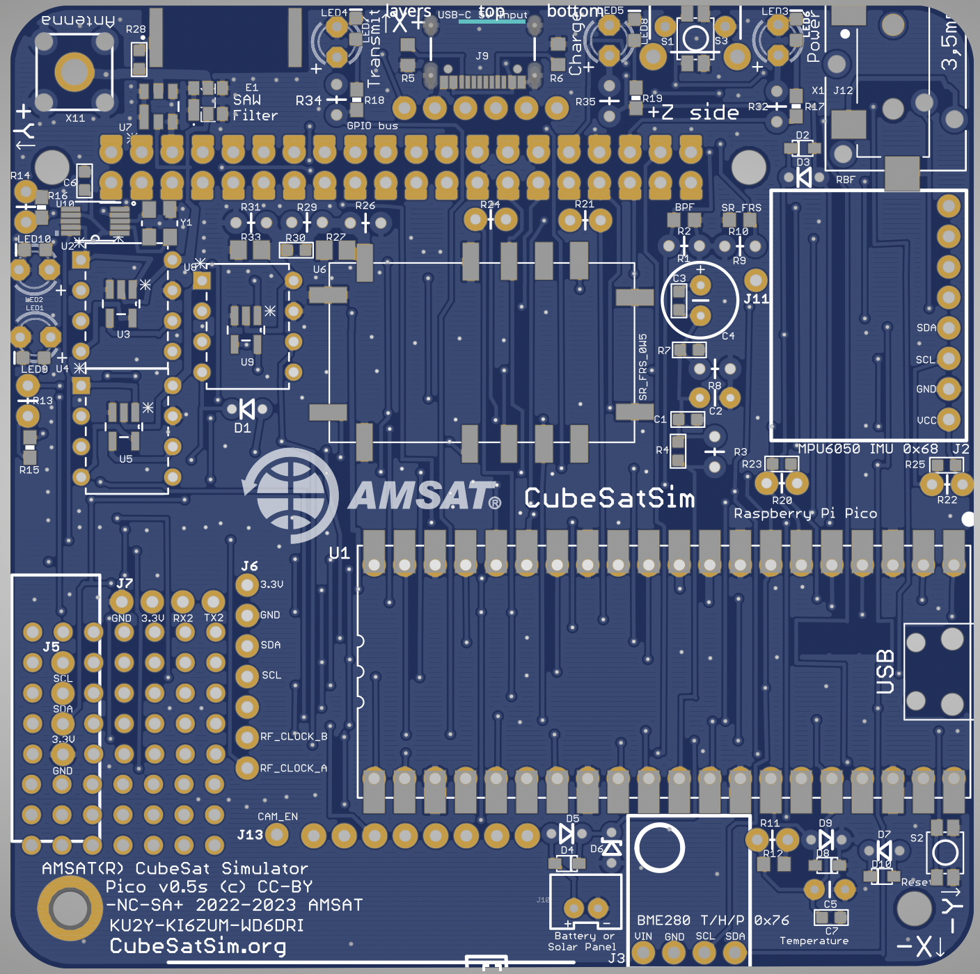
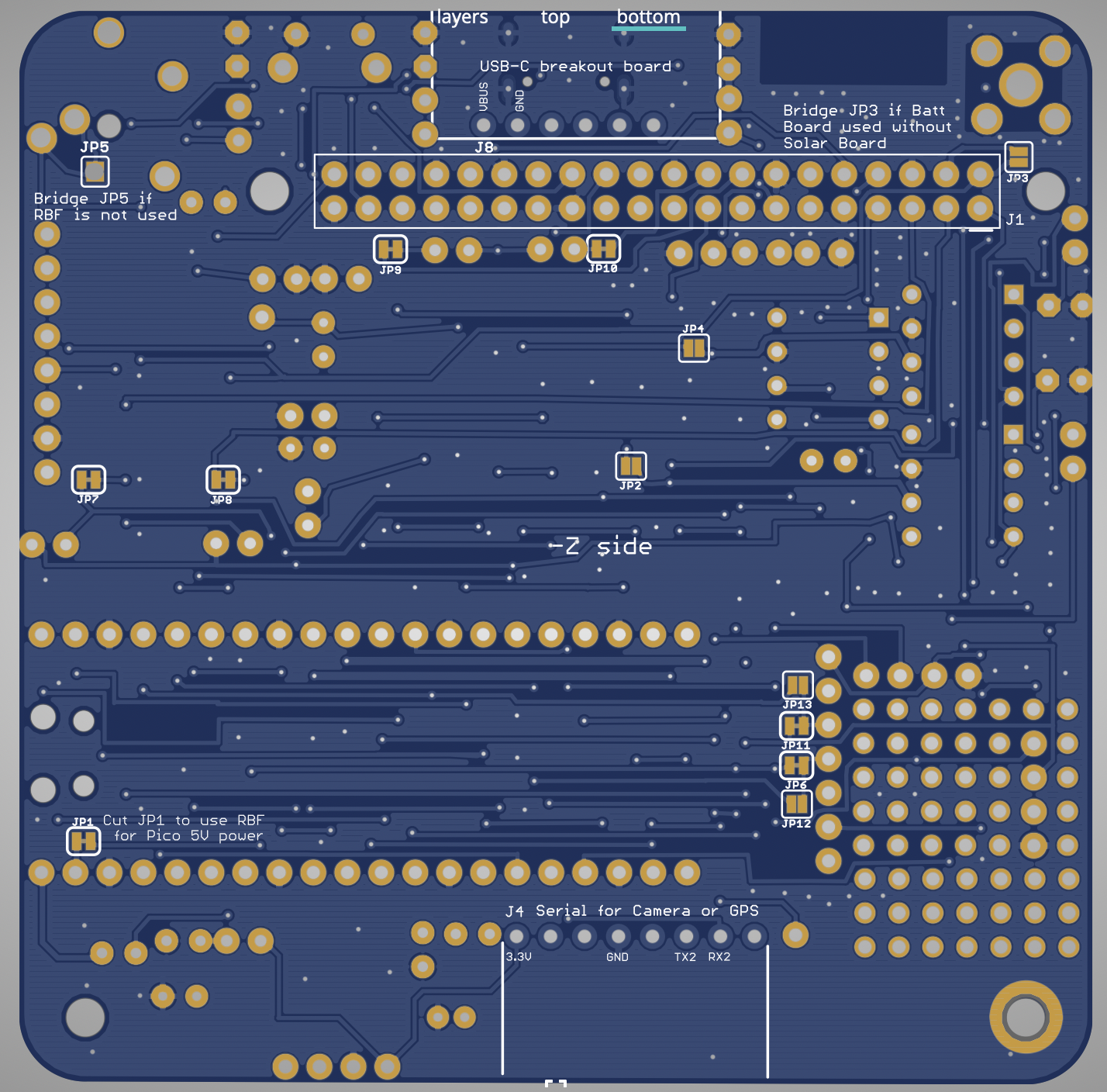
Here is the Pico PCB v0.5s:


The grey in the images indicates where solder paste is to be applied. Note that the Pico processor U1 is mounted on sockets, not SMD soldered, so no paste is applied to these pins.
The optional SMD components D5, J12, and LED6 - LED10 are not mounted, so no paste is applied to these pads.
You will need these tools:
- Safety glasses (to protect eyes while soldering or trimming leads)
- Solder Rework Station (a fine tip soldering iron and a hot air wand)
- Fine solder
- Solder paste
- Reflow oven
- Flux pen
- Tweezers
- Needle nose pliers (to bend leads and hold parts)
The best way to do SMD soldering is to use solder paste with a stencil and run the board through a reflow oven. The instructions here will cover this approach.
An alternative approach is to solder each component individually with an iron or hot air. This approach is covered here for the v0.2 PCB: Pico v0.2 SMD Instructions
Start with your SMD stencil setup. You will need three blank PCBs of the same thickness, a backing board, the metal stencil, and some tape to secure it all together:

The PCB should slide in securely but not be loose. When the stencil is laid on top, you should only see the PCB pads. Apply the solder paste to the stencil and spread.

Spread until all pads are evenly filled:

Open the stencil and remove the PCB:

The components can be mounted in any order. Sometimes it is easier to attach the PCB to cardboard or a board so you don't have to touch the PCB to move it around.
Resistors do not have a polarity. Check resistor values before mounting and double check with a meter if you are unsure.
All capacitors except one do not have a polarity.
Some of the components have a polarity - those components will be shown here.
The polarity of diode D8 is indicated by a white line on the component:

Here's how it looks mounted on the PCB:

The polarity of diodes D2 and D10 is indicated by a white line on the component:

Here's how they look installed on the PCB:


The polarity of the chip antenna E1 is indicated by the writing on it. The side closest to the Y of YAGEO should be on the left as shown here:

The capacitor C2 has a polarity indicated by a bar on the component:

The bar should face up on the PCB as shown here:

The crystal Y1 has one pad which is notched as you can see from this view of the bottom:

If you flip it upside down, it looks like this:

It then mounts on the PCB like this:

The SAW BPF also has one pad which is larger than the others:

If you flip it over, it looks like this:

Here's how it looks installed:

The clockgen IC U10 has a dot marking pin one, which should be down and to the right:

Be careful not to use too much solder paste otherwise the pins will be bridged. Here is how it looks installed:

The SR_FRS FM Module U6 is difficult to handle since it is too large for tweezers. Also, try to align the pins with the pads. When mounted, it looks like:

Here is the complete board:

Here is the board after running through the reflow oven:

Finally, solder the through hole components including:

- Red, Green and Blue LEDs: LED5, LED3, LED2, LED1, LED 4.
- Stacking GPIO header J1 (mounted on the bottom of the PCB)
- Female sockets 1x20 for the Pico U1
- Female socket 1x8 for the BME280 J3
- Female socket 1x4 for the MPU6050 J2
- Switch S1
- RBF Switch X1
- Female socket 1x8 right angle J4 (mounted on the bottom of the PCB)
Once all these components are installed, the board can be powered up via the Pico micro USB and you should see the red and green LEDs on, the blue LED come on when transmitting.

Note that if you have a Pico W, you will not see a green LED blinking on the Pico.
With power to the USB-C connector on the top, with the RBF 3.5mm plug installed, you should only see the red LED on:

With the RBF plug removed, you should see all the LEDs as before:

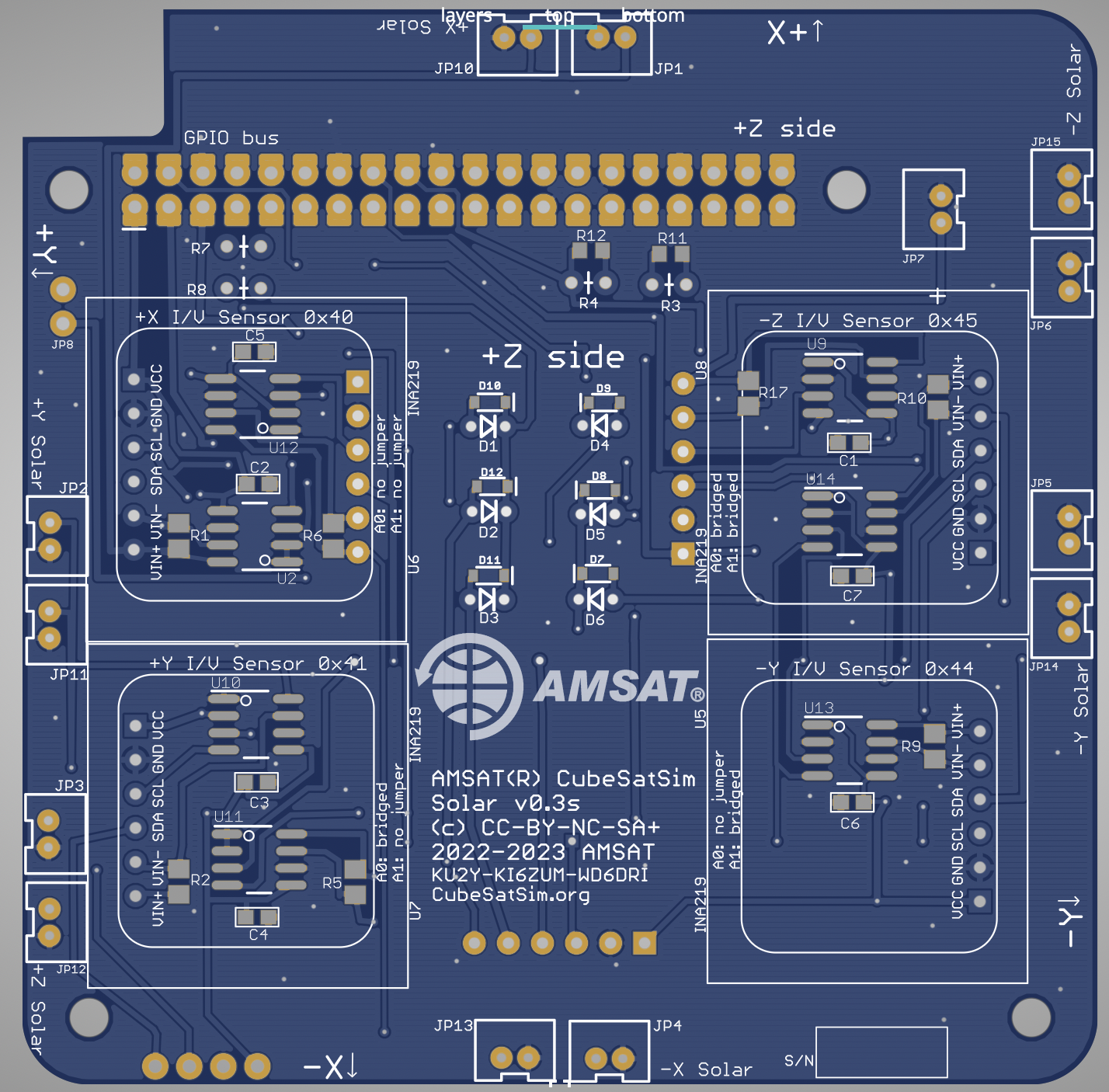
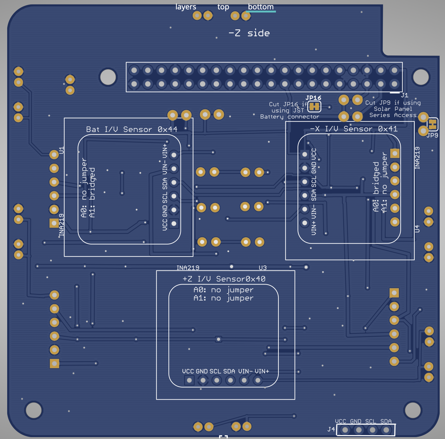
Here is the Solar PCB v0.3s:


Start with the stencil and apply solder paste:


Here's how the board looks with solder paste applied:

Resistors and capacitors on the board do not have any polarity.
The diodes have a bar to indicate polarity:

Here's how they look installed with correct polarity:

The INA219 ICs have a bar to indicate the side with pin 1:

The PCB also has a bar to indicate pin 1, for example here:

Here's how all the ICs look installed:

Here's all the components before going through the reflow oven:

Next solder the Through-Hole components:

- Stacking GPIO header J1 (mounted on the bottom of the PCB)
- JST 2.0 connectors JP1 - JP6, JP10 - JP15
Here's how the board looks finished:
