A reincarnation of eP32, a 32-bit CPU by Dr. Ting. However, deviating from the long linage of eForth, it uses Java Bytecode as the internal instruction set and hence the name J. After developing CPUs for decades, Dr. Ting, in a write up for eJsv32 manual, he concluded the following
Which instruction set will be the best and to survive to the next century? Looking around, I can see only one universal computer instruction set, and it is now gradually prevailing. It is Java.
Responding to the invitation from Don Golding of CORE-I FPGA project AI & Robotics Group, Dr. Ting dedicated the last few months of his life on developing eJ32. Based on his VHDL eP32, the transcoded SystemVerilog set was completed but never has the chance been fully verified or validated in time before his passing.
I appreciate that Dr. Ting took me in his last projects and considered me one of his student. Though a trained software engineer, who have never worked on any FPGA before, I felt overwhelmingly obligated to at least carry his last work to a point that future developers can benefit from the gems of his life's effort.
My goal is to make the learning journey of building eJ32 as an example of designing and implementing an FPGA CPU regardless whether Java will be the prevailing ISA or not.
Currently, though eJ32 has been successfully simulated with Dr. Ting's test cases but yet synthesized on the targeted ICE40. It will take sometime to realize for lack of hardware design knowledge on my part. If interested in a fully functional Forth CPU, Dr. Ting's origial eP16 or Bowman's J1a are both great to start. Anyway, for a kick, here're what I've done for eJ32 so far.
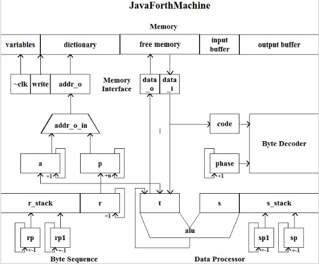
- keep Dr. Ting's original code in ~/orig/eJsv32k
- keep Dr. Ting's documentation in ~/docs
- create ~/source/eJ32.sv as the main core
- update mult/divide/shifter/ushifter modules using simple *, /, <<
- externalize ram_memory.v module, use spram.sv and eJ32_if.sv for Lattice iCE40UP FPGA
- create a dictionary ROM from eJsv32.hex, 8K bytes, sourcing from original ej32i.mif (see source/README for details)
- add ~/test/dict_setup.sv, use $fload to install memory map (i.e. eJsv32.hex)
- add top module ~/test/outer_tb.sv to drive memory block, dict_setup, and inner interpreter eJ32
- add eJ32.vh, use enum for opcodes replacing list of parameters
- refactor eJ32.sv
- use common tasks and macros to reduce verbosity
- removed phaseload, aselload which are always 1'b1
- add many $display for tracing (and my own understanding)
- fix divider, add one extra cycle for TOS update before next instruction
- modulize into a 2-bus hierachical design
- use iCE40 EBR (embedded block memory) for 64-deep data and return stacks (was 32-deep)
- use EBR as ROM which is populated from hex image file (contains 3.4K eForth + 1K test cases)
- add JTAG, HSOSC, RGB in top module for Map, P&R,...
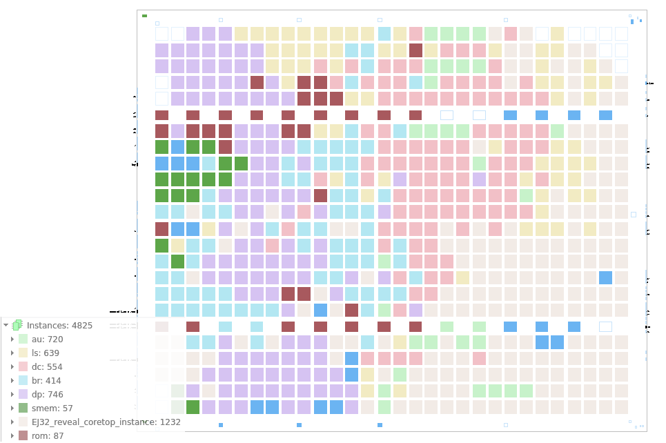
| module | desc | components | LUTs/freq area |
LUTs/freq timing |
LUTs (47op) |
note | err |
|---|---|---|---|---|---|---|---|
| ROM | eForth image (3.4K bytes) | 8K bytes onboard ROM | 49 166.5 |
17 272.9 |
49 | 8-bit 16 EBR blocks |
|
| RAM | memory | 128K bytes onboard RAM | 48 2392.3 |
49 2392.3 |
48 | 8-bit pseudo-dual port |
|
| AU | arithmetic unit | ALU and data stack | 928 31.3 |
939 31.3 |
1755 | 2 EBRs | |
| BR | branching unit | program counter and return stack | 425 26.8 |
435 31.0 |
333 | 2 EBRs | |
| DC | decoder unit | state machines | 194 34.7 |
193 39.8 |
211 | divider patch | |
| DP | data processor unit | shr/shl/mul/div | 731 17.9 |
621 21.3 |
439 | 3 DSPs | |
| LS | load/store unit | memory and buffer IO | 522 54.0 |
530 47.4 |
201 | 54.0 | |
| CTL | control bus | TOS, code, phase | NA | NA | NA | interface not synthsized |
|
| EJ32 | top module | JTAG,HSOSC,RGB | 3905 11.4 |
3721 11.4 |
NA | JTAG=778 | slow... |
To refactor:
- make all outputs registered (sync sub-blocks)
- compare to eP16 design
- tune DP for 24MHz (i.g. set_multicycle_path on divider, immd register)
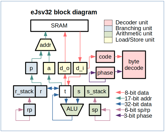
- combine IU (instruction unit, in eJ32.sv) and BR
- BR add R (top of return stack) register to help EBR slow path
- AU add S (NOS) register to help EBR slow path
- break IF (instruction fetch) off LS
- break RR (t Register Read), WB (t, s Write Back) off AU
- study pipelining hazards
- structure - RR-WB, BR-IU
- data - p_inc, divz, s
- control - p (and exception)
- Install Lattice Radiant 3.0+ (with Free license from Lattice, comes with ModelSim 32-bit)
- clone this repository to your local drive
- Open eJsv32.rdf project from within Radiant
- Compile, Synthesis if you really want to, and simulate (with ModelSim)
| section | starting address | note |
|---|---|---|
| eForth image | 0x0000 | loaded from ROM |
| Input buffer | 0x1000 | no RX unit yet, loaded from ROM |
| Output buffer | 0x1400 | no TX unit yet |
- targeting only Lattice iCE40UP FPGA for now
- No serial interface (i.e. UART, SPI, ..)
- fixed validation cases hardcoded in TIB (at 'h1000)
- output writes into output buffer byte-by-byte (starting at 'h1400)
- 33-cycle soft divider (iCE40 has no hardware divider)
- No Map or Route provided
- Data and return stacks
- 64-deep
- use iCE40 EBR, embedded block memory, pseudo dual-port, Lattice generated netlist, with negative edged clock
- eForth image (3.4K)
- use iCE40 EBR as ROM
- loaded from ROM into RAM during at start-up (8K cycles)
- The design works OK on ModelSim
- Core ~2.9K LUTs which should fit in iCE40 (3K or 5K)
- ModelSim COLD start - completed
- v1 - 10K cycles, ~/docs/eJ32_trace.txt
- v2 - 10K cycles, ~/docs/eJ32v2_trace_20240108.txt
- ModelSim Dr. Ting's 6 embeded test cases - completed
- v1 - 600K+ cycles OK, ~/docs/eJ32_trace_full_20220414.txt.gz (from Dr. Ting's)
- v1 - 520K+ cycles OK, ~/docs/eJ32_trace_full_20231223.txt.gz (before modulization)
- v2 - 520K+ cycles OK, ~/docs/eJ32v2_trace_full_20240117.txt.gz (after modulization)
For the 6 test cases Dr. Ting gave, they take ~520K cycles.
| units | instructions (in K) | total cycles(in K) | note |
|---|---|---|---|
| AU only | 108 | 159 | mostly 1 cycle |
| BR only | 10 | 20 | jreturn |
| DP only | 0.4 | 14 | idiv,irem,imul,ishr |
| LS only | 24 | 112 | b/i/saload |
| AU + BR | 50 | 145 | |
| AU + LS | 14 | 69 |
So, within the total cycles. details here
- Only 47 total opcodes are used.
- Arithmetic takes about 1/3, mostly 1-cycle except bipush(2), pop2(2), dup2(4)
- Branching takes about 1/3, all 3-cycle except jreturn 2-cycle.
- Load/Store takes about 1/3, all multi-cycles (avg. 5/instructions)
- check P16 variant here
- learn how to really Map, Place & Route (here's the 1st try with JTAG + RGB, at 11.4MHz)
- Consider memory clock at higher freq i.g. 4x CPU's (so 32-bit returns in 1 cycle)
- Consider i-cache + branch prediction to reduce branching delay
- Consider 32-bit and/or d-cache to reduce load/store delay
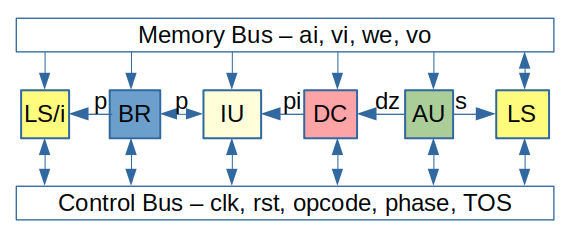
- Consider Pipelined design (see bus design above)
- Note: Pure combinatory module (no clock) returns in 1 cycle but lengthen the path which slows down the max frequency. Pipeline does the opposite.
- build hardwired control table
- learn how to resolve Hazards
- learn CSR + Hyper Pipelining
- IceStorm, open source synthesis, https://clifford.at/icestorm
- Project-F, https://github.com/projf/projf-explore
- Verilator + SDL2, https://projectf.io/posts/verilog-sim-verilator-sdl/
- Verilator
- part-1~4 https://itsembedded.com/dhd/verilator_1/ ...
- SpinalHDL
- RISC-V Pipeline design https://passlab.github.io/CSE564/notes/lecture09_RISCV_Impl_pipeline.pdf
- 20220110 - Chen-hanson Ting: eJsv32k.v in Quartus II SystemVerilog-2005
- 20220209 - Chochain: rename to eJ32 for Lattice and future versions
- 20230216 - Chochain: consolidate ALU modules, tiddy macro tasks
- 20231216 - Chochain: modulization flat to hierarchical (v2.0)
- 20240108 - Chochain: use EBR for data/return stacks and eForth image