VideoCore IV BCM2835 Overview
This page contains a set of diagrams taken from various patents covering the BCM2835 or related families of multimedia processor devices. It is provided here for those interested in gaining a high level understanding quickly. Not all information may be directly relevant to the BCM2835 but reading between the lines should work a treat.
The content is reproduced from the patents under the assumption that they are a matter of public record and the patents contain no explicit statement of copyright (as is required for copyright protection in a USA filed patent).
Ok, so lets get rolling... What exactly is in the BCM2835?
- ARM1176JZ-F Applications Processor nominally clocked at 700 MHz.
- ARMv6 architecture.
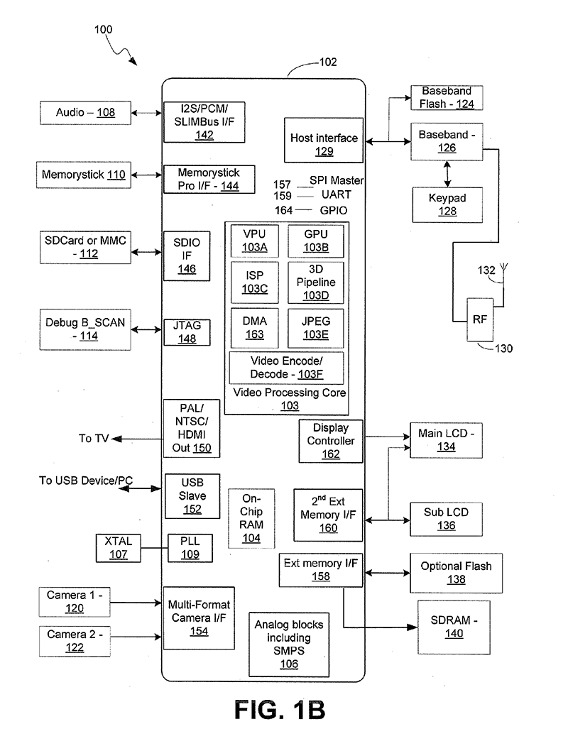
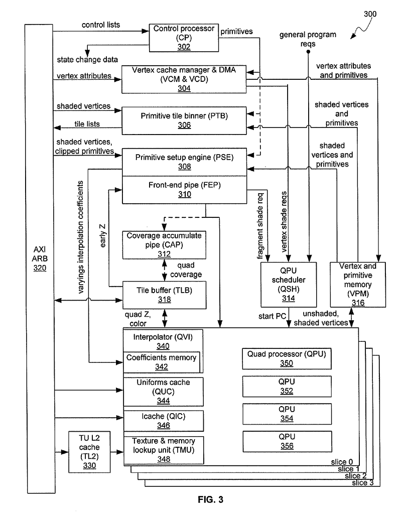
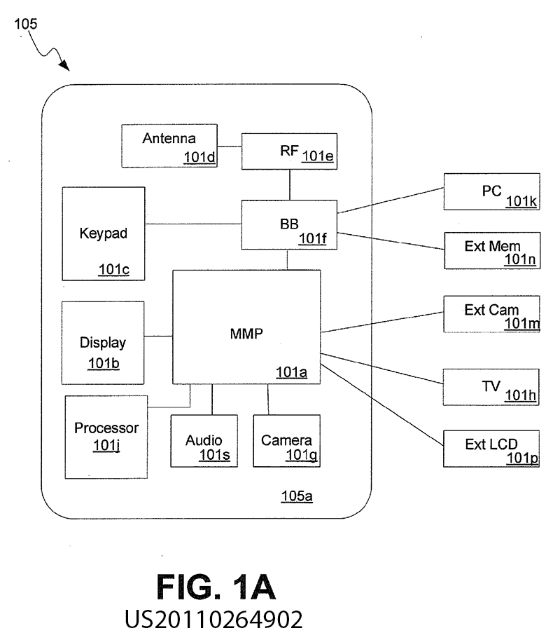 (from Patent US20110264902)
- Low Power ARM1176JZ-F Applications Processor
- Dual Core VideoCore IV® Multimedia Co-Processor
- Using the vector unit, it can software decode VP6, VP7, VP8, RV, Theora, WMV9 at DVD resolutions.
- Low power, high performance OpenGL-ES® 1.1/2.0 VideoCore GPU. 1 Gigapixel per second fill rate.
- 24 Gigaflops of floating point performance (3x4x8x250MHz)
- Hardware block assisting JPEG encode and decode.
- 1080p30 Full HD HP H.264 Video Encode/Decode
- The GPU can hardware decode H264, MPEG1/2/4, VC1, AVS, MJPG at 1080p30.
- Advanced Image Sensor Pipeline (ISP) for up to 20-megapixel cameras operating at up to 220 megapixels per second
At http://www.raspberrypi.org/phpBB3/viewtopic.php?f=2&t=3042#p40366, dom writes:
L2 cache.
The GPU has a 128K 4 way set associative cache.
The default configuration is to dedicate it to the GPU, and the ARM bypasses it.
There's a number of reasons for this. Obviously sharing the cache will mean both the ARM and GPU get less benefit due to evictions and additional cache misses.
The L2 cache is designed for the GPU. It is closer the GPU (in clock cycles), so a cache hit provides more benefit for the GPU than the ARM.
The L2 cache is outside the ARM's MMU. That means a contiguous (virtual) buffer that is significantly less than 128K may not be able to be fully cached (worst case a single 20K buffer may end up in 5 conflicting 4K pages).
I've measured latency from ARM to:
L1 cache hit 7ns.
SDRAM as 128ns (for a SDRAM page hit).
SDRAM as 167ns (for a SDRAM page miss).
L2 cache hit 68ns.
L2 cache miss 153ns (for a SDRAM page hit)
L2 cache miss 192ns (for a SDRAM page miss)
(this is actually with ARM at 600MHz. Overclocking options obviously will reduce these numbers. My latency measurment is a sequence of ld r0,(r0) instructions, which may include some processor pipeline stalls).
So with L2 cache enabled from ARM a cache hit is about twice as fast. A cache miss is significantly slower than an access with L2 disabled. Some use cases will be faster with L2 enabled, but not all. Obviously if the GPU is working hard through the cache, the ARM will be seeing more misses.
So, that's why L2 cache is disabled from ARM. However it is still worth investigating whether it speeds up some use cases (e.g. X GUI with browser).