VideoCore IV Programmers Manual
Official VideoCore IV 3D Architecture Reference Guide
Disclaimer:

This is a independent documentation project based on a combination of static
analysis and trial and error on real hardware.  This work is 100% independent
from and not sanctioned by or connected with Broadcom or its agents.
No Broadcom documents or materials were used beyond those publicly available.

This work was undertaken and the information provided for non commercial use on
the expectation that hobbyists of all ages will find the details useful for
understanding and working with their Raspberry Pi hardware.

The hope is that Broadcom will be flattered by the interest in the device and
understand the benefits of opening up understanding to a larger audience of
potential customers and developers.

Broadcom should be commended with making their SoC available for a project as
exciting as the Raspberry Pi.

No copyrighted materials are contained in this repository.  Diagrams from patents
have been included here but they are believed to not be covered by copyright.

See:
http://en.wikipedia.org/wiki/Copyright_on_the_content_of_patents_and_in_the_context_of_patent_prosecution).
Contributors:
- Phire
- Matt
- Booto
- Herman
- David
- thubble
- mgottschlag
- eizo-san
- Sarah Ocean
- NOTE: This is in a very early state and is of limited accuracy. This is an early release by request.
- Mnemonics wont match official VideoCore IV due to this being an independent work. That said we have tried to match up names with the existing names in the Alphamosaic and Broadcom patents.
- Not all instructions have been tested at this stage.
- Mnemonics have been aligned vaguely with ARM, AVR given the expected audience (Raspberry Pi users). They are subject to change.
- Vector instructions are a work in progress, and all information is very preliminary (even moreso than the rest of this document).
- A good cross reference of instructions semantics is Mathias's emulation work at https://github.com/mgottschlag/vctools/blob/master/vcdb/_instructions.yaml and related files.
The scalar processor can load and store byte (b), half word (h or s16/u16) and word (u32) quantities to/from memory.
The scalar processor uses 2's complement encoding for arithmetic operations and IEEE 754 single precision floating point format (binary32) for floating point operations.
The vector (or multimedia) instructions can process up to 16 quantities at a time in a SIMD fashion. The vector unit has a 64x64 register bank - that can be addressed in horizontal or vertical fashion to select a horizontal or vertical slice of 16 adjacent values.
The processor has at least 3 states configured by bits 31 and 29 of the processor status register sr (r30):
- Supervisor mode, active when bit 29 of sr is set.
- Exception mode, active when bit 29 of sr is clear.
- User mode, active when bit 31 of sr is set and bit 29 is set.
According to the BCM2835 ARM Peripherals manual, address ranges are:
  0x00000000 - 0x3fffffff  ; L1 and L2 cached
  0x40000000 - 0x7fffffff  ; L2 cache coherent (non allocating)
  0x80000000 - 0xbfffffff  ; L2 cached only
  0xc0000000 - 0xffffffff  ; Direct uncached
Responders are:
  0x00000000 - 0x1fffffff  ; SDRAM
  0x20000000 - 0x20007fff  ; Boot (OTP or) ROM.
  0x7e000000 - 0x7effffff  ; IO
16Kb Icache, 32bytes per cache line. Involved in the branch prediction logic on the VPU.
As far as I understand, the VPU does not cache a data cache. Register definitions seem to support this theory.
128Kb 4 way set associative cache.
General purpose 32-bit registers:
- r0, r1, ..., r15 are used for both integer, logical and floating point operations.
Extended 32-bit registers:
- r16, r17, ..., r24 are available for integer, logical and floating point operations in a range of instructions.
- r24 (gp) the global pointer is typically used to refer to the base of the data section.
Special purpose 32-bit registers:
- r25 (sp) the stack pointer.
- r26 (lr) the link register for saving return address on execution of branch-and-link instructions.
- r27
- r28 (esp) the stack pointer for exception handlers. During an exception handler r25 refers to r28 and the original r25 is not accessible. In user mode r28 is not accessible and is mapped to r27.
- r29 (tp) thread/core pointer. Typically holds a pointer to per thread/core data structure.
- r30 (sr) the processor status register (UIS- ---- ---- ---- ---- ---- --cb ZNCV).
- V overflow flag (set by cmp, cmn, btest, and fcmp).
- C carry flag (set by cmp, cmn, btest, and fcmp).
- N negative flag (set by cmp, cmn, btest, and fcmp).
- Z zero flag (set by cmp, cmn, btest, and fcmp).
- CB Vector Register file column base/offset.
- S supervisor flag,
- I interrupt flag,
- U user flag.
- r31 (pc) the program counter holding the current execution address.
Processor Control Registers (according to hardware_vc4.h in BRCM driver release):
- p0 to p31, access via the
mov p<d>, r<a>ormov r<d>, p<a>instructions. - p0 is PRFPXCS for scalar floating point exception control.
- p1 is PRCANARY for stack canary (when enabled).
- p2 to p9 are unassigned.
- p10 [B0] is PRPOWCTL.
- p11 [B0] is PRTIMCTL for Closely Coupled Timer Control (core and sleep timers).
- p12 [B0] is PRCORTIM for Core Timer Result.
- p13 is PRSLPTIM for Sleep Timer Result.
- p14 is PROWCNT for Count of outstanding writes.
- p15 is PRORCNT for Count of outstanding reads.
- p16-p31 are single-bit mutexes, shared between the two VPUs.
- p16 is PRSPINL used by spinlock, a lightweight mutex.
- p17 is Used by vcos_quickslow_mutex on ThreadX in existing start.elf's.
- p18 - p31 are unassigned.
Note: In contrast to many processors, only a small subset of instructions update the Condition Code flags. In particular cmp, cmn, btest, and fcmp set the flags. In contrast, addcmpb, ror, shl, lsr, asr do not set the flags.
The program counter isn't typically accessed directly, due to pipeline restrictions. Direct access using the standard instruction forms will typically raise an illegal instruction exception. Instead alternate ld/st/lea encodings exist to reference addresses relative to the pc.
Special instruction encodings for ld/st are availible for relative r0, r24, sp and pc addressing.
- Parameters in r0-r5
- Return result in r0
- Preserve registers r6+
- Caller saves r0-r5 (if needed), Callee saves and restores r6+.
The Vector Register file is a 2d array of 64x64 8 bit integer cells or elements. A horizontal vector is composed of 16 horizontal adjacent cells, whilst a vertical vector is made of 16 vertically adjacent cells. The vectors are just "names" for collections of the underlying integer cells, so it should be understood that the same cells may be appear in multiple different different horizontal and vertical vectors.
A single cell P(y,x) is located at horizontal position x and vertical position y:
Vector Register File (as byte cells):
    P(0,0)  P(0,1) ... P(0,63)
    P(1,0)  P(1,1) ... P(1,63)
    ...     ...        ...
    P(63,0) P(63,1)... P(63,63)
To support 16 and 32 bit quantities, the underlying 8-bit cells can be combined:
- The name
P(y,x)denotes a single 8-bit cell at coordinates (y,x). - The name
PX(y,x)denotes a 16-bit value at coordinates (y,x). It is composed of two 8-bit cells. - The name
PY(y,x)denotes a 32-bit value at coordinates (y,x). It is composed of four 8-bit cells.
These values are mapped (in a 16-byte strided little endian manner) as follows:
-
P(y,x)an 8-bit cell, value:P(y,x) -
PX(y,x)a 16-bit cell, value:P(y,x) | (P(y,x+16)<<8) -
PY(y,x)a 32-bit cell, value:P(y,x) | (P(y,x+16)<<8) | (P(y,x+32)<<16) | (P(y,x+48)<<24)
As the 16 and 32 bit values come from multiple cells, there are limitations on their horizontal positions:
-
PX(y,x)is limited to 0 <= x <= 15, or 32 <= x <= 63 -
PY(y,x)is limited to 0 <= x <= 15
The array can be imagined as wrapping, so that P(y,x) should be seen as referring to P(y&63,x&63). This is important when it comes to considering vectors extending beyond the edge of the array (such as H(63,0)).
Another consideration for PX() is that whilst we talk about cell PX(y,32), strictly speaking it is encoded with x=16, but we write PX(y, 32) for simplifying visualizing the arrangement.
Register addressing modes exist to reference horizontal, or vertical slices of 16 values to be operated on in parallel in a SIMD manner. The 16 values may be accessed as either 8, 16, or 32 quantities. Note that the vector unit operates on 16 input values, the only difference being the bit width of each value.
H(y,x)   Horizontal row of int8           [P(y,x), P(y,x+1), ..., P(y,x+15)]
V(y,x)   Vertical column int8             [P(y,x), P(y+1,x), ..., P(y+15,x)]

HX(y,x)  16-bit Horizontal row of int16   [PX(y,x), PX(y,x+1), ..., PX(y,x+15)]
VX(y,x)  16-bit Vertical column of int16  [PX(y,x), PX(y+1,x), ..., PX(y+15,x)]

HY(y,x)  32-bit Horizontal row of int32   [PY(y,x), PY(y,x+1), ..., PY(y, x+15)]
VY(y,x)  32-bit Vertical column if int32  [PY(y,x), PY(y+1,x), ..., PY(y+15,x)]
Possible alternate names for registers are:
H(y,x),  as HB(y,x), or H8(y,x)
HX(y,x), as HH(y,x), or H16(y,x)
HY(y,x), as HL(y,x), or H32(y,x)
V(y,x),  as VB(y,x), or V8(y,x)
VX(y,x), as VH(y,x), or V16(y,x)
VY(y,x), as VL(y,x), or V32(y,x)
Here B means byte (8 bits), H means halfword (16 bits), and L means longword (32 bits).
When referring to vector registers in instructions we may use the convenience notation D, A, B or Rd, Ra, Rb, or R(yd, xd) etc to refer to a vector register in the Destination, Source A, or Source B position. eg:
vadd D, A, B
vadd Rd, Ra, Rb
vadd R(yd,xd), R(ya, xa), R(yb, xb)
vadd V(yd, xd), H(ya, xa), H(yb, xb)
When performing a read access to V(y,x)+0x1000, the vector to be read as:
 [P(y,x), P(y,x), ..., P(y,x)], rather than [P(y,x), P(y+1,x), ..., P(y+15,x)]

Likewise H(y,x)+0x1000, the vector is read as:
 [P(y,x), P(y,x), ..., P(y,x)], rather than [P(y,x), P(y,x+1), ..., P(y, x+15)]
This replicating alias applies to 16 and 32 bit quantities as well. It provides and efficient mechanism for loading all active lanes with the same value. The lower order 12 bits of of the vector position still contribute a valid offset, eg:
mov r0, ( (1<<12) | (2<<6) | (1<<0) )
vmov HX(0,0), HX(0, 16)+r0
results in HX(0,0) = [ PX(2,17), PX(2,17), ..., PX(2,17) ]
For efficient implementation of palettized pixel formats or gamma conversions etc, the vector unit supports a 1024 byte lookup table. This allows a 16 element vector to lookup values in parallel. It has sufficient size for 4x 256 byte lookup tables for mapping 8 bit values to 8 bit, or 2x 512 byte tables for mapping 8 bit values to 16 bits, or 1x 1024 byte table for mapping 8 bit values to 32 bits.
Instructions are encoded in 16, 32, 48 or 80 bits. The basic pattern is:
1111 1xxx xxxx xxxx y:32 z:32    vector80
1111 0xxx xxxx xxxx y:32         vector48
1110 xxxx xxxx xxxx y:32         scalar48
1xxx xxxx xxxx xxxx y:16         scalar32
0xxx xxxx xxxx xxxx              scalar16
Instructions can be thought of as sequences of little endian 16 bit words. The byte order is thus:
vector80  1 0,  3 2,  5 4,  7 6,  9 8
vector48  1 0,  3 2,  5 4
scalar32  1 0,  3 2,
scalar16  1 0
The exception is the scalar48 instructions which can be thought of as a little endian 16 bit word, followed by a little endian 32 bit word:
scalar48 1 0, 5 4 3 2
Condition codes for conditional instruction execution are encoded as a 4-bit field:
Bits    Comment     Meaning        Name

0000    Simple      Equal          eq
0001    Simple      Not Equal      ne
0010    Unsigned    C set, <       cs/lo    Note inverted sense of carry from ARM.
0011    Unsigned    C clear, >=    cc/hs    Note inverted sense of carry from ARM.
0100    Simple      N set          mi
0101    Simple      N clear        pl
0110    Simple      V set          vs
0111    Simple      V clear        vc
1000    Unsigned    >              hi
1001    Unsigned    <=             ls
1010    Signed      >=             ge
1011    Signed      <              lt
1100    Signed      >              gt
1101    Signed      <=             le
1110    Simple      Always
1111    Simple      Never          f
Arithmetic and logical operations are encoded as a 4, 5, or 6 bit field depending on the instruction. The table below gives the full 6-bit operation codes; to map an instruction to an operation code, use the following:
4-bit  oooo  -> 0oooo0, ie. only 16 operations are available (mov, add, mul, and so forth)
5-bit ooooo  -> 0ooooo, ie. only the first 32 operations are available
6-bit oooooo -> oooooo, ie. all operations are available
The operations are encoded as follows:
000000    mov      rd, ra              rd = ra                               Move.
000001    cmn      rd, ra              ZNCV = cc(rd + ra)                    Compare values by addition.
000010    add      rd, ra              rd = rd + ra                          Add
000011    bic      rd, ra              rd = rd & ~ra                         Logical bit clear.
000100    mul      rd, ra              rd = rd * ra                          Multiply.
000101    eor      rd, ra              rd = rd ^ ra                          Logical Exclusive Or.
000110    sub      rd, ra              rd = rd - ra                          Subtract.
000111    and      rd, ra              rd = rd & ra                          Logical And.
001000    not      rd, ra              rd = ~ra                              Not / 1s Complement.
001001    ror      rd, ra              rd = rotate_right(rd, ra)             Rotate right.
001010    cmp      rd, ra              ZNCV = cc(rd - ra)                    Compare values.
001011    rsub     rd, ra              rd = ra - rd                          Reverse subtract.
001100    btest    rd, ra              Z = (rd & bit(ra)) == 0               Bit test.
001101    or       rd, ra              rd = rd or ra                         Logical or.
001110    bmask    rd, ra              rd = rd & mask(ra)                    Mask left most bits.
001111    max      rd, ra              rd = max(ra, rd)                      Maximum.
010000    bitset   rd, ra              rd = rd | bit(ra)                     Bit set.
010001    min      rd, ra              rd = min(ra, rd)                      Minimum.
010010    bitclear rd, ra              rd = rd & ~bit(ra)                    Bit clear.
010011    addscale rd, ra << 1         rd = rd + (ra << 1)                   Add scaled by 2.
010100    bitflip  rd, ra              rd = rd ^ bit(ra)                     Bit flip.
010101    addscale rd, ra << 2         rd = rd + (ra << 2)                   Add scaled by 4.
010110    addscale rd, ra << 3         rd = rd + (ra << 3)                   Add scaled by 8.
010111    addscale rd, ra << 4         rd = rd + (ra << 4)                   Add scaled by 16.
011000    signext  rd, ra              rd = sign_extend(rd & mask(ra))       Mask left most bits and sign extend.
011001    neg      rd, ra              rd = -ra                              Negate.
011010    lsr      rd, ra              rd = rd >> ra                         Logical shift right.
011011    msb      rd, ra              rd = msb(ra)                          Position of most significant 1 bit, (msb(0)==-1)
011100    shl      rd, ra              rd = rd << ra                         Logical shift left.
011101    brev     rd, ra              rd = reverse(rd) >> (32-ra)           Reverse bits and shift right.
011110    asr      rd, ra              rd = rd >> ra                         Arithmetic shift right.
011111    abs      rd, ra              rd = abs(ra)                          Absolute value.
100000    mulhd.ss rd, ra, rb          rd = (ra * rb) >> 32                  High half of 32x32 -> 64 bit product; ra, rb are both signed
100001    mulhd.su rd, ra, rb          rd = (ra * rb) >> 32                  High half of 32x32 -> 64 bit product; ra is signed, rb is unsigned
100010    mulhd.us rd, ra, rb          rd = (ra * rb) >> 32                  High half of 32x32 -> 64 bit product; rb is signed, ra is unsigned
100011    mulhd.uu rd, ra, rb          rd = (ra * rb) >> 32                  High half of 32x32 -> 64 bit product; ra, rb are both unsigned
100100    div.ss   rd, ra, rb          rd = (ra / rb)                        Divide; ra, rb are both signed
100101    div.su   rd, ra, rb          rd = (ra / rb)                        Divide; ra is signed, rb is unsigned
100110    div.us   rd, ra, rb          rd = (ra / rb)                        Divide; rb is signed, ra is unsigned
100111    div.uu   rd, ra, rb          rd = (ra / rb)                        Divide; ra, rb are both unsigned
101000    adds     rd, ra, rb          rd = saturate32(ra + rb)
101001    subs     rd, ra, rb          rd = saturate32(ra - rb)
101010    shls     rd, ra, rb          rd = saturate32(ra << rb)
101011    clipsh   rd, rb              rd = saturate16(rb)
101100    addscale rd, ra, rb << 5     rd = ra + (rb << 5)
101101    addscale rd, ra, rb << 6     rd = ra + (rb << 6)
101110    addscale rd, ra, rb << 7     rd = ra + (rb << 7)
101111    addscale rd, ra, rb << 8     rd = ra + (rb << 8)
110000    count    rd, rb              rd = count(rb)
110001    subscale rd, ra, rb << 1     rd = ra - (rb << 1)
110010    subscale rd, ra, rb << 2     rd = ra - (rb << 2)
110011    subscale rd, ra, rb << 3     rd = ra - (rb << 3)
110100    subscale rd, ra, rb << 4     rd = ra - (rb << 4)
110101    subscale rd, ra, rb << 5     rd = ra - (rb << 5)
110110    subscale rd, ra, rb << 6     rd = ra - (rb << 6)
110111    subscale rd, ra, rb << 7     rd = ra - (rb << 7)
111000    subscale rd, ra, rb << 8     rd = ra - (rb << 8)

Where:
  Unary operations ignore ra, ie '<op> rd, ra, rb' behaves as 'rd = <op> rb'
  Operations 57 (111001) to 63 (111111) are undefined and raise a 0x03 exception.
  All bit shifts counts are modulo 32 (ie. masked with &31).
  bit(x) =  1 << x
  mask(x) = bit(x)-1
  saturate16(x) = min(0x7fff, max(-0x8000, x))
  saturate32(x) = min(0x7fffffff, max(-0x80000000, x))
  count(x) = number of 1 bits in x.
The width of memory operations is encoded as follows:
  ww is 00 for ld/st for u32 operations.
  ww as 01 for ldh/sth for u16 operations.
  ww as 10 for ldb/stb for u8 operations.
  ww as 11 for ldsh/ldsb for s16/s8 load operation.
NOTE: What would apparently decode as the nonsensical stsh is infact ldsb (load 8 bit signed).
0000 0000 0000 0000    bkpt                Halt/Breakpoint

0000 0000 0000 0001    nop                 No operation

0000 0000 0000 0010    sleep               (provisional)
0000 0000 0000 0011    user                (provisional) Enter user mode.

0000 0000 0000 0100    ei                  Enable interrupts
0000 0000 0000 0101    di                  Disable interrupts

0000 0000 0000 0110    cbclr               Clear vector column base ie SR[5:4] = 0
0000 0000 0000 0111    cbadd1              Add 1 to vector column base ie SR[5:4]+=1
0000 0000 0000 1000    cbadd2              Add 2 to vector column base ie SR[5:4]+=2
0000 0000 0000 1001    cbadd3              Add 3 to vector column base ie SR[5:4]+=3

0000 0000 0000 1010    rti                 Return from interrupt, ie. sr = *sp++; pc = *sp++;

0000 0000 001d dddd    swi rd              Software Interrupt.  Raise interrupt 0x20+(rd&0x1f)

0000 0000 010d dddd    b rd                Branch to address in rd, ie. pc = rd.
0000 0000 011d dddd    bl rd               Save pc to lr and branch to target, ie. pc = rd.

0000 0000 1000 dddd    switch.b rd         Table branch byte.  pc = pc + 2*(*(s8 *)(pc+rd))
0000 0000 1010 dddd    switch rd           Table branch short. pc = pc + 2*(*(s16 *)(pc+rd))

0000 0000 111d dddd    version rd          Get cpu version and core number.

0000 0001 11uu uuuu    swi u               Software Interrupt.  Raise interrupt 0x20+u&0x1f
Memory Operations:
0000 0010 0bbm mmmm    ldm rb-rm,(sp++)    Load registers from stack (highest first).
0000 0010 1bbm mmmm    stm rb-rm,(--sp)    Store registers to stack (lowest first).
0000 0011 0bbm mmmm    ldm rb-rm,pc,(sp++) Load registers from stack and final value into pc.
0000 0011 1bbm mmmm    stm rb-rm,lr,(--sp) Store lr followed by registers onto stack.

                                           where:
                                           - rb is r0, r6, r16, or r24 for bb == 00, 01, 10, 11.
                                           - rm = (rb+m)&31

                                           If sp is stored, then the value after the store is stored.
                                           If mmmmm is 31 and pc/lr are stored/loaded, then no register
                                           but pc/lr is stored/loaded ("stm lr/ldm pc"). The same
                                           applies at least to "stm r24-r7, lr, (--sp)".

0000 010o oooo dddd    ld   rd, (sp+o*4)   Load from memory relative to stack pointer.
0000 011o oooo dddd    st   rd, (sp+o*4)   Store to memory relative to stack pointer.

0000 1ww0 ssss dddd    ld<w>   rd, (rs)    Load from memory.
0000 1ww1 ssss dddd    st<w>   rd, (rs)    Store to memory.

0001 0ooo oood dddd    add  rd, sp, o*4    rd = sp + o*4

0001 1ccc cooo oooo    b<cc>  $+o*2        Branch on condition to target.

0010 uuuu ssss dddd    ld  rd, (rs+u*4)    rd = *(rs + u*4)
0011 uuuu ssss dddd    st  rd, (rs+u*4)    *(rs + u*4) = rd
Arithmetic and Logical Operations:
010 op:5 s:4 d:4     Rd = Rd op Ra         Register with Register logical and arithmetic operations.
011 op:4 u:5 d:4     Rd = Rd op u          Register with Immediate logical and arithmetic operations.
Add an increment then branch conditionally based on a comparison:
1000 cccc aaaa dddd 00ss ssoo oooo oooo    addcmpb<cc> rd, ra, rs, $+o*2   rd += ra; if (rd <cc> rs) branch
1000 cccc iiii dddd 01ss ssoo oooo oooo    addcmpb<cc> rd, i, rs, $+o*2    rd += i;  if (rd <cc> rs) branch
1000 cccc aaaa dddd 10uu uuuu oooo oooo    addcmpb<cc> rd, ra, u, $+o*2    rd += ra; if (rd <cc> u) branch
1000 cccc iiii dddd 11uu uuuu oooo oooo    addcmpb<cc> rd, i, u, $+o*2     rd += i;  if (rd <cc> u) branch
Long conditional branch and branch and link:
1001 cccc 0ooo oooo oooo oooo oooo oooo    b<cc> $+o*2                     if (<cc>) branch to target.
1001 oooo 1ooo oooo oooo oooo oooo oooo    bl $+o*2                        Save pc to lr and branch to target.
Memory access:
# Conditional with indexed
1010 0000 ww0 d:5 a:5 c:4 00 b:5           ld<w>.<cc> rd, (ra + rb << w)   if (<cc>) rd = *(ra+rb*width)
1010 0000 ww1 d:5 a:5 c:4 00 b:5           st<w>.<cc> rd, (ra + rb << w)   if (<cc>) *(ra+rb*width) = d

# 12 bit displacement
1010 001o ww0 d:5 a:5 o:11                 ld<w> rd, (ra+o)                rd = *(ra+o)
1010 001o ww1 d:5 a:5 o:11                 st<w> rd, (ra+o)                *(ra+o) = rd

# Conditional with pre decrement
1010 0100 ww0 d:5 a:5 c:4 00 0 0000        ld<w>.<cc> rd, (--ra)           if (<cc>) rd = *--ra
1010 0100 ww1 d:5 a:5 c:4 00 0 0000        st<w>.<cc> rd, (--ra)           if (<cc>) *--ra = rd

# Conditional with post increment
1010 0101 ww0 d:5 a:5 c:4 00 0 0000        ld<w>.<cc> rd, (ra++)           if (<cc>) rd = *ra++
1010 0101 ww1 d:5 a:5 c:4 00 0 0000        st<w>.<cc> rd, (ra++)           if (<cc>) *ra++ = rd

# 16 bit displacement
1010 1000 ww 0 d:5 o:16                    ld<w> rd, (r24+o)              rd = *(r24+o)
1010 1000 ww 1 d:5 o:16                    st<w> rd, (r24+o)              *(r24+o) = rd
1010 1001 ww 0 d:5 o:16                    ld<w> rd, (sp+o)               rd = *(sp+o)
1010 1001 ww 1 d:5 o:16                    st<w> rd, (sp+o)               *(sp+o) = rd
1010 1010 ww 0 d:5 o:16                    ld<w> rd, (pc+o)               rd = *(pc+o)
1010 1010 ww 1 d:5 o:16                    st<w> rd, (pc+o)               *(pc+o) = rd
1010 1011 ww 0 d:5 o:16                    ld<w> rd, (r0+o)               rd = *(r0+o)
1010 1011 ww 1 d:5 o:16                    st<w> rd, (r0+o)               *(r0+o) = rd
Arithmetic and Logical Operations
1011 00 op:5 d:5 i:16                      <op> rd, i                     rd = rd op i
1011 01 s:5 d:5 i:16                       add rd, rs, i                  rd = rs + i
1011 1111 111 d:5 o:16                     add rd, pc, o                  rd = pc + o
Conditional Arithmetic and Logical Operations:
1100 0 op:6 d:5 a:5 c:4 00 b:5             <op>.<cc> rd, ra, rb           if (<cc>) rd = rd op ra
1100 0 op:6 d:5 a:5 c:4 1 i:6              <op>.<cc> rd, ra, i            if (<cc>) rd = ra op i
where 'op' is taken from the arithmetic operations table above and 'cc' from the condition code table. 'i' is treated as either signed or unsigned, depending on the operation.
Floating Point Operations:
1100 100 fop:4 d:5 a:5 c:4 00 b:5          <fop>.<cc> rd, ra, rb          if (<cc>) rd = ra fop rb
1100 100 fop:4 d:5 a:5 c:4 1 i:6           <fop>.<cc> rd, ra, i           if (<cc>) rd = ra fop float6(i)
Where:
  fop is an operation according to the 4 bit floating point operation table:
    fadd, fsub, fmul, fdiv, fcmp, fabs, frsub, fmax,
    frcp, frsqrt, fnmul, fmin, fceil, ffloor, flog2, fexp2

  cc is a condition code test (see condition code table);
    eq,ne ,cs/lo, cc/hs, mi, pl, vs, vc, hi, ls, ge, lt, gt, le

  float6(x) converts a 6 bit binary number to float (1 sign bit, 3 bit exponent, 2 bit mantissa)
      float float6(imm) {
        uint32_t b = 0;
        if (imm & 0x20) {
            b |= 0x80000000;
        }
        int exponent = (imm >> 2) & 0x7;
        if (exponent != 0) {
            b |= (exponent + 124) << 23;
            int mantissa = imm & 0x3;
            b |= mantissa << 21;
        }
        return *(float *)&b;
      }
Floating Point Integer Conversion:
1100 101 0 000 d:5 a:5 c:4 00 b:5          ftrunc.<cc> rd, ra, sasl rb    if (<cc>) rd = (int)(ra*pow(2,rb))
1100 101 0 000 d:5 a:5 c:4 1 i:6           ftrunc.<cc> rd, ra, sasl i     if (<cc>) rd = (int)(ra*pow(2,i))
1100 101 0 001 d:5 a:5 c:4 00 b:5          floor.<cc> rd, ra, sasl rb     if (<cc>) rd = (int)floor(ra*pow(2,rb))
1100 101 0 001 d:5 a:5 c:4 1 i:6           floor.<cc> rd, ra, sasl i      if (<cc>) rd = (int)floor(ra*pow(2,i))
1100 101 0 010 d:5 a:5 c:4 00 b:5          flts.<cc> rd, ra, sasr rb      if (<cc>) rd = ((float)(int)ra)/pow(2,rb)
1100 101 0 010 d:5 a:5 c:4 1 i:6           flts.<cc> rd, ra, sasr i       if (<cc>) rd = ((float)(int)ra)/pow(2,i)
1100 101 0 011 d:5 a:5 c:4 00 b:5          fltu.<cc> rd, ra, sasr rb      if (<cc>) rd = ((float)(uint)ra)/pow(2,rb)
1100 101 0 011 d:5 a:5 c:4 1 i:6           fltu.<cc> rd, ra, sasr i       if (<cc>) rd = ((float)(uint)ra)/pow(2,i)

Where:
  sasl is an arithmetic shift left by a signed amount (ie negative shifts, shift to the right).
  sasr is an arithmetic shift right by a signed amount (ie negative shifts, shift to the left).
Processor Control Register Access:
1100 1100 000 d:5 0000 0000 000 a:5        mov pd, ra                     pd = ra
1100 1100 001 d:5 0000 0000 000 a:5        mov rd, pd                     rd = pa
Memory access:
1110 0000 0000 0000 u:32                   j u                                Jump to target.
1110 0001 0000 0000 o:32                   b $+o                              Branch to target.
1110 0010 0000 0000 u:32                   jl u                               Save pc to lr and jump to target.
1110 0011 0000 0000 o:32                   bl $+o                             Save pc to lr and branch to target.

1110 0101 000 d:5 o:32                     add rd, pc, o                      rd = pc + o

1110 0110 ww 0 d:5 s:5 o:27                ld<w>  rd, (rs+o)                  Load from address rs+o to rd+o
1110 0110 ww 1 d:5 s:5 o:27                st<w>  rd, (rs+o)                  Store from rd to address rs+o

1110 0111 ww 0 d:5 11111 o:27              ld<w>  rd, (pc+o)                  Load pc relative.
1110 0111 ww 1 d:5 11111 o:27              st<w>  rd, (pc+o)                  Store pc relative.
Arithmetic and Logical operations with 32 bit immediate:
1110 10 p:5 d:5 u:32                       <op> rd, u                         rd = rd op u
1110 11 s:5 d:5 u:32                       add rd, rs, u                      rd = rs + u
Reminder: the scalar48 instructions are best thought of as a little endian 16 bit word, followed by a little endian 32 bit word. This is in contrast to all other instruction encodings which are best thought of as a series of little endian 16 bit words.
There are two major groups of vector instructions - Vector Memory operations and Vector Data operations.
Vector memory operations allow the transfer of register contents to and from memory or the 1 Kb lookup table.
Vector data operations allow computation between two 16 element vectors writing the result back to a third 16 element vector. Vector data operations may also perform scalar register update (SRU), accumulation (ACC), repeated execution (REP2, ..., REP r0) and lane selection based on condition codes.
Vector instructions are encoded in a full 80-bit format or a compact 48-bit format. Instructions in the compact format support fewer options, but generate less icache pressure.
Refer to the diagram below which has been taken from Patent application EP1320029.
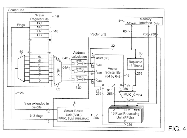
- Two 16 element long vectors A and B are fetched from the vector register file.
- The Pixel Processing Units ( PPUs ) execute the same operation in parallel ( SIMD ) on the 16 element pairs. D[i] = A[i] op B[i] for i=0...15. Despite the name they may be used for a variety of purposes in addition to graphics.
- The result is written back to the register file.
Instructions can be repeated 2, 4, 8, 16, 32, 64 or a conditional number of times. A single instruction repeated 64 times (using REP 64 ) would be working on a total of 64x16, or 1024 elements.
Each Pixel Processing Unit has a set of 3 condition flags, Z, N, C which can be updated by executing an instruction (using the SETF flag). In subsequent instructions Pixel Processing Units may be directed to disable themselves based on the state of the condition flags. eg. The IFNZ modifier would mean only enable PPUs with a zero flag that is clear.
After calculation the PPUs may accumulate results over a number of instructions using an accumulator or ACC located in each PPU. Result values may either be added or subtracted to the accumulator, and the accumulated value may be used to replace the result value for write back to the vector register file.
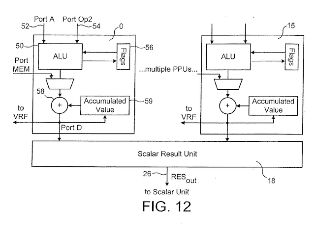
The scalar result unit is used to optionally update a scalar register (r0...r7) with a value computed from the vector result. For instance SUM, IMIN, IMAX, MAX modifiers may be used to calculate the sum, or index of minimum element, or index of maximum element, or the maximum value from the 16 vector result values.
Quoting from US Patent Application 20030159023 ( http://www.google.com/patents/US20030159023 ):
vadd H(0,0), H(0,0), #116 horizontally contiguous 8-bit pixels (“H”) are read from the top left (0,0) of the VRF. The PPUs add the immediate value 1 to each and the results are written back to the same location (only the least significant 8 bits are returned because the destination register is an 8-bit register). No flags are changed, and no accumulation occurs.
vadd −, H(0,0), #0 SETFvadd H(0,0), H(0,0), #1 IFNThese instructions process sixteen horizontally contiguous 8-bit values (“H”) located at (0,0) in the VRF. The first instruction sets the PPU flags according to the values there (but does not need to write the values back anywhere—hence “−” as the destination); the second instruction adds one only to the negative values (“IFN”), leaving the others alone.
vadd H(0++, 16), H(0++, 0), #0 REP 16The 16×16 block of 8-bit pixels at (0,0) in the VRF is copied to (0,16) (adding zero is being used here just to copy registers). The H indicates that we read and write 16 horizontally contiguous pixels from the VRF. Upon each of the 16 repetitions (“REP 16”), the x-component of the source and destination are each incremented by 1 (“++”), that is 1 byte.
NOTE: This looks like a typo, I think it should say "...the y-component of the source and destination [position] are each increment by 1 ("++"), ...
vdist −, H(0++,0), H(0++,16) REP 16 CLRA ACC SUM r0Computes the distance (absolute difference) between two 16×16 pixel blocks. Each repetition computes the 16 distances between two sets of 16 values and each PPU adds the answer to its own accumulator (“ACC”), which also means these accumulated values become the PPU outputs. Finally we sum these 16 values and write the result, now the total distance between the two blocks, into scalar register r0 (“SUM r0”). The CLRA modifier clears the accumulators on the initial repetition, and is the only modifier to behave differently on subsequent repetitions (on which it does nothing).
NOTE: "CLRA ACC" and "SUM r0" seem mutually exclusive given the bit encodings below. It may be the ability to perform both has been removed since the patent was written.
vsub −, H(0++,0)+r0, r1 REP 16A constant value taken from register r1 (in the SRF) is subtracted from every pixel in an arbitrary 16×16 block. The scalar register r0 (in the SRF) supplies the address of the top left corner of the block to be processed. When used in this way, the 6 least significant bits of r0 indicate the x-offset of the block, and the next 6 bits indicate the y-offset.
This is much easier to understand than it first appears...
- Values Baddr, Aaddr and Daddr are determined from the instruction and the contents of referenced scalar registers. Addressing modes include:
- R(y, x), absolute vector register reference. Also R(y++, x), and R(y, x++).
- R(y, x) + rs, relative vector register reference where an offset from an absolute position is encoded as a 6:6 bit number in rd. Also R(y++,x)+rs, and R(y,x++)+rs.
- R(0, 0) + rs, absolute vector register reference in scalar register, encoded as 6:6 as above. Also R(0++,0)+rs, and R(0,0++)+rs.
- rb, a 32 bit value from a scalar register (only available for vector operand B).
- rb+#s9, a 32 bit value calculated from the scalar register and constant (only available for vector operand B).
- #s16, a 16 bit immediate value (only available for vector operand B).
-
- , discard value (only available for vector operand D).
- For vector load instructions, MEM is fetched from the 32 bit address Baddr: MEM = memory[ Baddr ].
- Vectors A and B are taken from the vector register file: A = VRF[ Aaddr ], B = VRF[ Baddr ].
- For vector store instructions, A is written to memory: memory[ Baddr ] = A.
- OP2 is selected as either B or Baddr : OP2 = choose(B, { Baddr, Baddr, ..., Baddr}).
- The pixel processing units (PPU) perform their calculations: D = vop(A, OP2, MEM)
- If this is the first cycle of a repeated instruction the accumulator ACC is optionally reset to 0.
- Accumulation occurs as specified by the instruction, one of:
- No accumulation.
- Accumulation: tmp = ACC + D, optional: D = tmp, optional: ACC = tmp.
- Subtraction: tmp = ACC - D, optional: D = tmp, optional: ACC = tmp.
- Optional: Vector result write back: VRF[ Daddr ] = D.
- Optional: Scalar Result Unit: rs = SRU(D), where SRU maps a vector to a scalar value, eg. sum of values: SUM(), index of minimum value: IMIN(), index of maximum value: IMAX().
- If the instruction has the SETF bit set, then the conditional codes of each PPU is updated.
- Increment Aaddr, Baddr, Daddr according to the instruction specification: this is often an optional step to the adjacent vector position below (horizontal vectors), or to the right (vertical vectors). When Baddr is used as a memory address, it is typically a memory stride to step to the next storage position (a value from a scalar register): eg. (rb+#offset+=rs) would mean start at rb+offset and add rs for each instruction repetition.
- If the repeat count or condition is not yet exhausted then goto 2.
Note the expression D = vop(A, OP2, MEM), means the evaluation of a 16 element wide vector expression. In the case of conditional execution: IFZ, IFNZ, IFN, IFNN, IFC, IFNC, then individual pixel processing units may be disabled based on the state of each units condition flags (zero, negative, carry).
Vector instruction arguments are normally 10 bits long. The first 4 bits describe the nature of the argument as well as the 2 high order bits of X coordinate; the last 6 bits give the exact Y coordinate (row) in the case of horizontal vectors, or the 2 bits of high order Y coordinate and 4 bits of low order X coordinate (column) in the case of vertical vectors:
0 x5 x4 v y5 y4 xy3 xy2 xy1 xy0

Horizontal:
0000 y5 y4 y3 y2 y1 y0     H(y, 0)
0010 y5 y4 y3 y2 y1 y0     H(y, 16)
0100 y5 y4 y3 y2 y1 y0     H(y, 32)
0110 y5 y4 y3 y2 y1 y0     H(y, 48)
1000 y5 y4 y3 y2 y1 y0     HX(y, 0)
1010 y5 y4 y3 y2 y1 y0     HX(y, 32)
1100 y5 y4 y3 y2 y1 y0     HY(y, 0)

Vertical:
0001 y5 y4 x3 x2 x1 x0     V(y, 0+x)
0011 y5 y4 x3 x2 x1 x0     V(y, 16+x)
0101 y5 y4 x3 x2 x1 x0     V(y, 32+x)
0111 y5 y4 x3 x2 x1 x0     V(y, 48+x)
1001 y5 y4 x3 x2 x1 x0     VX(y, 0+X)
1011 y5 y4 x3 x2 x1 x0     VX(y, 32+x)
1101 y5 y4 x3 x2 x1 x0     VY(y, 0+x)

Other:
1110      For destination discard result, as first source ignore value,
          as second source use coordinate as scalar value.
1111
The limitations on the 48 bit instructions are:
- vector references are either all horizontal or all vertical, ie the direction of the A and B vectors matches the destination D.
- Accumulation (ACC) is not possible,
- Scalar Register Update (SRU) is not possible,
- Vector coordinates are limited.
Operations supported: vld (vector load), vst (vector store), vlookup (vector gather), vindexwrite (vector gather), vreadlut, vwritelut.
Memory Instructions variants (48 bit) are:
v<mop><width> H(yd,xd)[+rs], H(ya,xa)[+rs], (rb) [SETF]
v<mop><width> V(yd,xd)[+rs], V(ya,xa)[+rs], (rb) [SETF]
v<mop><width> H(yd,xd)[+rs], H(ya,xa)[+rs], H(yb,xb)[+rs]
v<mop><width> V(yd,xd)[+rs], V(ya,xa)[+rs], H(yb,xb)[+rs]
v<mop><width> H(yd,xd)[+rs], H(ya,xa)[+rs], #immediate [SETF] [IFZ|IFNZ|IFN|IFNN|IFC|IFNC]
v<mop><width> V(yd,xd)[+rs], V(ya,xa)[+rs], #immediate [SETF] [IFZ|IFNZ|IFN|IFNN|IFC|IFNC]
Encoded as:
1111 00 mop:5 width:2 rs:3 d:10 a:10 z0 111 F:1 rb:6   v<mop><width> Rd[+rs], Ra[+rs], (rb) [SETF]
1111 00 mop:5 width:2 rs:3 d:10 a:10 z0 b:10           v<mop><width> Rd[+rs], Ra[+rs], Rb[+rs]
1111 00 mop:5 width:2 rs:3 d:10 a:10 z1 P:3 F:1 i:6    v<mop><width> Rd[+rs], Ra[+rs], #i [SETF] [IFZ|IFNZ|IFN|IFNN|IFC|IFNC]
Where is B (8), H (16), or L (32), and determines the size of transfers to memory.
  width:2 is 00 to read/write vector elements as bytes.
  width:2 is 01 to read/write vector elements as 16 bits.
  width:2 is 10 to read/write vector elements as 32 bits.
  width:2 is 11 acts as 00, but is probably reserved for future use.
- What would in an 80 bit instruction be the direction bits of A and B are used to choose if a single scalar register should be added to the location ie vadd H(0,0), H(1,0)+rs, H(2,0)+rs;
- For D, bit 11 of the instruction decides if should be added. eg. vadd H(0,0)+rs, H(1,0), H(2,0)
- When B is an immediate value, bits P:3 are used to select a lanes via flag predication.
- When B is an address from a scalar register value, or an immediate value, bit F:1 is used to update ALU flags.
Seven types of memory operation have been determined:
Load/Store/Scatter/Gather:

00000  ld            Load vector from memory.  D[i] = *(rb+i*width)
00001  lookupmh      Gather values.            D[i] = *(rb+ACCH[i]*width)
00010  lookupml      Gather values.            D[i] = *(rb+ACC[i]*width)

00100  st            Store vector to memory.   *(rb+i*width) = A[i]
00101  indexwritemh  Scatter values.           *(rb+ACCH[i]*width) = A[i].
00110  indexwriteml  Scatter values.           *(rb+ACC[i]*width) = A[i].

Lookup Table - A 1024 byte lookup-table for fast lookups.

01000  readlut       Lookup values in LUT.     D[i] = lut(B[i]*width). eg. readlut V(0,0), -, V(16,0)
01001  writelut      Write values to LUT.      lut(B[i]*width) = A[i]. eg. writelut 0, V(0,0), (r0)

Accumulator Access:

11000  readacc       Read from accumulator.    D[i] = ACC[i]>>> B[i]

Width:
  ld, lookup (gather), st, indexwrite (scatter), readlut, writelut,
  all support 8, 16, 32 bit operations (00, 01, 10).  Width (11) seems to be a no-op.

For readacc, the width field behaves differently.
  00  reads acc without saturation
  01  reads acc saturating to 32 bits
  10  no-op
  11  reads acc saturating to 16 bits
Note that load/store, like all vector operations, always operate on 16 values. So loading 32-bit values will load 64 bytes from memory at once.
Data Instructions (48 bit) have a 6-bit opcode, and have the following variants:
v<op><X> H(yd,xd)[+rs], H(ya,xa)[+rs], (rb) [SETF]
v<op><X> V(yd,xd)[+rs], V(ya,xa)[+rs], (rb) [SETF]
v<op><X> H(yd,xd)[+rs], H(ya,xa)[+rs], H(yb,xb)[+rs]
v<op><X> V(yd,xd)[+rs], V(ya,xa)[+rs], H(yb,xb)[+rs]
v<op><X> H(yd,xd)[+rs], H(ya,xa)[+rs], #immediate  [SETF] [IFZ|IFNZ|IFN|IFNN|IFC|IFNC]
v<op><X> V(yd,xd)[+rs], V(ya,xa)[+rs], #immediate  [SETF] [IFZ|IFNZ|IFN|IFNN|IFC|IFNC]
Encoded as:
1111 01 X vop:6 rs:3 d:10 a:10 z0 111 F rb:6   v<op><X> Rd[+rs], Ra[+rs], (rb) [SETF]
1111 01 X vop:6 rs:3 d:10 a:10 z0 b:10         v<op><X> Rd[+rs], Ra[+rs], Rb[+rs]
1111 01 X vop:6 rs:3 d:10 a:10 z1 P:3 F:1 i:6  v<op><X> Rd[+rs], Ra[+rs], #i [SETF] [IFZ|IFNZ|IFN|IFNN|IFC|IFNC]
Where i is a 6-bit immediate value; zero-extended and supplied to each of the 16 parallel operations
The 1-bit field 'X' serves one of two purposes depending on the value of vop:
If vop < 48, then <X> is either 16 (aka. 'H', corresponding to X=0 in the instruction) or 32 (aka. 'L', corresponding to X=1), and determines the sign extension behaviour of source operands. ie. H (16), will sign extend the 16th bit when widening source operands. The operations <op> encoded with vop < 48 are:
000000 vmov Move.
000001 vbitplanes Make mask. Rd[i] = (Rb[i]&(1<<i)) ? -1 : 0.
000010 veven Pluck elements at even index. Rd[i] = (i<8) ? Ra[i*2] : Rb[(i-8)*2].
000011 vodd Pluck elements at odd index. Rd[i] = (i<8) ? Ra[1+i*2] : Rb[1+(i-8)*2].
000100 vinterl Interleave (alternate) lower 8 cells from Va & Vb. (Va[0], Vb[0], Va[1], Vb[1], ...)
000101 vinterh Interleave (alternate) upper 8 cells from Va & Vb. (Va[8], Vb[8], Va[9], Vb[9], ...)
000110 vbitrev Reverse bits and shift right. Rd[i] = reverse(Ra[i]) >> ((32-Rb[i])&31)
000111 vror Rotate right. Rd[i] = rotate_right(Ra[i], Rb[i]).
001000 vshl Logical shift left. Rd[i] = Ra[i] << (Rb[i]&31)
001001 vshls Saturating shift left. Rd[i] = shift_left_saturate(Ra[i], Rb[i]&31).
001010 vlsr Logical shift right. Rd[i] = Ra[i] >>> (R_b[i]&31)
001011 vasr Arithmetic shift right. Rd[i] = Ra[i] >> (Rb[i]&31)
001100 vsignshl Logical shift left by signed amount (ie logical shift right if Rb negative).
001101 vop13 Unused. R_d[i] = 0
001110 vsignasl Arithmetic shift left by signed amount (ie arithmetic shift right if Rb negative).
001111 vsignasls Saturating Arithmetic shift left by signed amount (ie arithmetic shift right if Rb negative).
010000 vand Bitwise AND R_d[i] = R_a[i] & R_b[i]
010001 vor Bitwise OR R_d[i] = R_a[i] | R_b[i]
010010 veor Bitwise XOR R_d[i] = R_a[i] ^ R_b[i]
010011 vbic Bitwise Clear R_d[i] = R_a[i] & ~(R_b[i])
010100 vcount Population count R_d[i] = (# of nonzero bits in R_a[i]) + (# of nonzero bits in R_b[i])
010101 vmsb Most significant bit position in Rd[i] = msb(Ra[i]|Rb[i])
010110 vop22 Unused. R_d[i] = 0
010111 vop23 Unused. R_d[i] = 0
011000 vmin Minimum R_d[i] = MIN(R_a[i], R_b[i])
011001 vmax Maximum R_d[i] = MAX(R_a[i], R_b[i])
011010 vdist Distance R_d[i] = ABS(R_a[i] - R_b[i])
011011 vdists Distance R_d[i] = MIN(MAX_INT<WIDTH>, ABS(R_a[i] - R_b[i]))
011100 vclip Unsigned Clamp R_d[i] = MAX(0, MIN(R_a[i], R_b[i])) ; eg R_d[i] = clamp(R_a[i], 0, R_b[i])
011101 vsign Sign. Rd[i] = sgn(Ra[i]) + Rb[i].
011110 vclips Signed Clamp R_d[i] = MAX(-R_b[i], MIN(R_a[i], R_b[i])) ; eg R_d[i] = clamp(R_a[i], -R_b[i], R_b[i])
011111 vtestmag Compare GE R_d[i] = (R_a[i] >= R_b[i]);
100000 vadd Add R_d[i] = R_a[i] + R_b[i]
100001 vadds Add with saturation R_d[i] = saturate(R_a[i] + R_b[i]) ; saturate to max/min int.
100010 vaddc Add with carry R_d[i] = R_a[i] + R_b[i] + C[i]
100011 vaddsc Add with saturation and carry R_d[i] = saturate(R_a[i] + R_b[i] + C[i]) ; saturate to max/min int.
100100 vsub Subtract R_d[i] = R_a[i] - R_b[i]
100101 vsubs Subtract with saturation R_d[i] = saturate(R_a[i] - R_b[i]) ; saturate to max/min int.
100110 vsubc Subtract with carry. R_d[i] = R_a[i] - R_b[i] - C[i]
100111 vsubsc Subtract with saturation and carry R_d[i] = saturate(R_a[i] - R_b[i]) ; saturate to max/min int.
101000 vrsub Rev. Subtract R_d[i] = R_b[i] - R_a[i]
101001 vrsubs Rev. Subtract with saturation R_d[i] = R_b[i] - R_a[i] ; saturate to max/min int.
101010 vrsubc Rev. Subtract with carry R_d[i] = R_b[i] - R_a[i] - C[i] ;
101011 vrsubsc Rev. Subtract with saturation and carry R_d[i] = R_b[i] - R_a[i] - C[i] ; saturate to max/min int.
101100 vop44 Unused. R_d[i] = 0
101101 vop45 Unused. R_d[i] = 0
101110 vop46 Unused. R_d[i] = 0
101111 vop47 Unused. R_d[i] = 0
For vop >= 48, <X> is not part of the instruction name; X instead seems to choose between two separate instruction tables, both based around different usages of a 16x16 -> 32 bit multiplier:
For X=0, the operations are:
110000    vmull.ss    Multiply      R_d[i] = R_a[i] * R_b[i]
110001    vmulls.ss   Saturated Multiply (signed - saturated to max/min int)
110010    vmulm.ss    Multiply middle word result (bytes 2:1) (only byte 2 signed)
110011    vmulms.ss   Saturated Multiply middle word result (signed - saturated to max/min int)
110100    vmulhd.ss   Multiply high word result (round-to-minus-inf/floor) (Ra and Rb signed)
110101    vmulhd.su   Multiply high word result (round-to-minus-inf/floor) (Ra signed, Rb unsigned)
110110    vmulhd.us   Multiply high word result (round-to-minus-inf/floor) (Ra unsigned, Rb signed)
110111    vmulhd.uu   Multiply high word result (round-to-minus-inf/floor) (Ra and Rb unsigned)
111000    vmulhn.ss   Multiply high word result with round-to-nearest/round (Ra and Rb signed)
111001    vmulhn.su   Multiply high word result with round-to-nearest/round (Ra signed, Rb unsigned)
111010    vmulhn.us   Multiply high word result with round-to-nearest/round (Ra unsigned, Rb signed)
111011    vmulhn.uu   Multiply high word result with round-to-nearest/round (Ra and Rb unsigned)
111100    vmulhdt.ss  Multiply high word result with round-to-zero/truncation (Ra and Rb signed)
111101    vmulhdt.su  Multiply high word result with round-to-zero/truncation (Ra signed, Rb unsigned)
111110    vop62.0     Unused. R_d[i] = 0
111111    vop63.0     Unused. R_d[i] = 0
For X=1, the operations multiply two 16-bit values (32-bit operands are truncated) and gives a full-width 32-bit result:
110000    vop48.1     Unused. R_d[i] = 0
110001    vop49.1     Unused. R_d[i] = 0
110010    vop50.1     Unused. R_d[i] = 0
110011    vop51.1     Unused. R_d[i] = 0
110100    vmul32.ss   Full-width multiply (Ra and Rb are 16-bit signed)
110101    vmul32.su   Full-width multiply (Ra is 16-bit signed, Rb is 16-bit unsigned)
110110    vmul32.us   Full-width multiply (Ra is 16-bit unsigned, Rb is 16-bit signed)
110111    vmul32.uu   Full-width multiply (Ra and Rb are 16-bit unsigned)
111000    vop56.1     Unused. R_d[i] = 0
111001    vop57.1     Unused. R_d[i] = 0
111010    vop58.1     Unused. R_d[i] = 0
111011    vop59.1     Unused. R_d[i] = 0
111100    vop60.1     Unused. R_d[i] = 0
111101    vop61.1     Unused. R_d[i] = 0
111110    vop62.1     Unused. R_d[i] = 0
111111    vop63.1     Unused. R_d[i] = 0
Note: When running code under the standard R-Pi firmware, the instructions with X=1 and vop >= 56 seem to cause the VPU to hang. What happens when running these instructions under custom firmware is unconfirmed.
Format of the first 48 bits is very similar to 48-bit (above). The main difference is that there are flags for repeating an instruction a specified number of times, and additional vector addressing modes.
v<mop><width> -, A(ya,xa)[+ra], imm16(rs+=rd) [REP] [IFxx] [SETF]
v<mop><width> D(yd,xd)[+rd], -, imm16(rs+=ra) [REP] [IFxx] [SETF]
v<mop><width> D(yd,xd)[+rd], A(ya,xa)[+ra], B(yb,xb)[+rb] [REP] [IFxx] [SETF]
v<mop><width> D(yd,xd)[+rd], A(ya,xa)[+ra], #immediate [REP] [IFxx] [SETF]

In the first two forms, rd or ra is added to the memory address at each repetition.
(But the instruction doesn't update the original register value).
Encoded as:
1111 10 mop:5 width:2 r:3 1110 rd:6 a:10 F 0 111 l:7 f_d:6 f_a:6 Ra_x:4 P:3 i:7 rs:4 i:2
1111 10 mop:5 width:2 r:3 d:10 1110 ra:6 F 0 111 l:7 f_d:6 f_a:6 Ra_x:4 P:3 i:7 rs:4 i:2
1111 10 mop:5 width:2 r:3 d:10 a:10 F 0 b:10 f_d:6 f_a:6 Ra_x:4 P:3 f_i:7 f_b:6
1111 10 mop:5 width:2 r:3 d:10 a:10 F 1 l:10 f_d:6 f_a:6 Ra_x:4 P:3 f_i:7 j:6

Where:
  imm = (i<<7) | l, or (j<<10) | l
  r:3    encodes the repetition modifier
6-bit opcode is denoted by 'v'. Same opcodes as 48-bit (see above).
v<op><X> D, A, B    [REP] [SETF] [IFxx] [SRU|ACC]
v<op><X> D, A, #imm [REP] [SETF] [IFxx] [SRU|ACC]

  REP  = ( REP2 | REP4 | REP8 | REP16 | REP32 | REP64 | REP r0)
  IFxx = ( IFZ | IFNZ | IFN | IFNN | IFC | IFNC )
  SRU  = ( SUMU | SUMS | IMIN | IMAX | MAX) ( r0 | r1 | ... | r7 )
  ACC  = [CLRA] ( UACC | UDEC | SACC | SDEC | UACCH | UDECH | SACCH | SDECH
                | UADD | USUB | SADD | SSUB | UADDH | USUBH | SADDH | SSUBH )
Encoded as:
1111 11 X v:6 r:3 d:10 a:10 F 0 b:10 f_d:6 f_a:6 Ra_x:4 P:3 f_i:7 f_b:6
1111 11 X v:6 r:3 d:10 a:10 F 1 k:10 f_d:6 f_a:6 Ra_x:4 P:3 f_i:7 j:6

Where:
  imm = (j<<10) | k
  r:3    encodes the repetition modifier
  X:1    encodes between 16 and 32 bit
  f_i:7  encodes the SRU or ACC settings.
  P:3    encodes lane predication.
Repetition r:3 is encoded:
000                 Do not repeat
001      REP2       Repeat 2x
010      REP4       Repeat 4x
011      REP8       Repeat 8x
100      REP16      Repeat 16x
101      REP32      Repeat 32x
110      REP64      Repeat 64x
111      REP r0     Repeat count comes from scalar register r0.
Each argument, in addition to the 10 bits described above, has an additional 6 bits which are flags describing additional options for the argument (repeat/increment, scalar, offset, etc.) The mnemonics (f_d, f_a, f_b) denote the flags for each argument. The usage of each bit is as follows:
5:2      Scalar register r0-r14, if required; otherwise, all 1's (ie r15 is not available)
1        If set, increment argument by 1 for each instruction repetition.
         Y coordinate is incremented if argument is horizontal; X coordinate if vertical.
0        If set use bits 5:4 of SR as a column offset for the vector reference.
         ie. P(y,x) becomes P(y,(x+cb*16)&63).
Ra_X, provides additional bits for the position of the Ra vector, allowing it to be fully specified.
3:0 Low order bits for xa in Ra(ya, xa).
So, the complete register encoding takes the form:
Vector destination D is defined by d:10, f_d:6
Vector source      A is defined by a:10, f_a:6 Ra_x:4
Vector source      B is defined by b:10, f_b:6

Generally d, a, b are of the form:

Horizontal:
  0000 y5 y4 y3 y2 y1 y0     H(y, 0)
  0010 y5 y4 y3 y2 y1 y0     H(y, 16)
  0100 y5 y4 y3 y2 y1 y0     H(y, 32)
  0110 y5 y4 y3 y2 y1 y0     H(y, 48)
  1000 y5 y4 y3 y2 y1 y0     HX(y, 0)
  1010 y5 y4 y3 y2 y1 y0     HX(y, 32)
  1100 y5 y4 y3 y2 y1 y0     HY(y, 0)
  111                        -

Vertical:
  0001 y5 y4 x3 x2 x1 x0     V(y, 0+x)
  0011 y5 y4 x3 x2 x1 x0     V(y, 16+x)
  0101 y5 y4 x3 x2 x1 x0     V(y, 32+x)
  0111 y5 y4 x3 x2 x1 x0     V(y, 48+x)
  1001 y5 y4 x3 x2 x1 x0     VX(y, 0+x)
  1011 y5 y4 x3 x2 x1 x0     VX(y, 32+x)
  1101 y5 y4 x3 x2 x1 x0     VY(y, 0+x)
  111                        -

Vector source A vectors take all their y bits from a:10, and their x bits from Ra_x, so this becomes:

Horizontal:
  0000 y5 y4 y3 y2 y1 y0     H(y, 0+Ra_x)
  0010 y5 y4 y3 y2 y1 y0     H(y, 16+Ra_x)
  0100 y5 y4 y3 y2 y1 y0     H(y, 32+Ra_x)
  0110 y5 y4 y3 y2 y1 y0     H(y, 48+Ra_x)
  1000 y5 y4 y3 y2 y1 y0     HX(y, 0+Ra_x)
  1010 y5 y4 y3 y2 y1 y0     HX(y, 32+Ra_x)
  1100 y5 y4 y3 y2 y1 y0     HY(y, 0+Ra_x)
  111                        -

Vertical:
  0001 y5 y4 y3 y2 y1 y0     V(y, 0+Ra_x)
  0011 y5 y4 y3 y2 y1 y0     V(y, 16+Ra_x)
  0101 y5 y4 y3 y2 y1 y0     V(y, 32+Ra_x)
  0111 y5 y4 y3 y2 y1 y0     V(y, 48+Ra_x)
  1001 y5 y4 y3 y2 y1 y0     VX(y, 0+Ra_x)
  1011 y5 y4 y3 y2 y1 y0     VX(y, 32+Ra_x)
  1101 y5 y4 y3 y2 y1 y0     VY(y, 0+Ra_x)
  111                        -
P:3, controls which vector lanes/elements are active.
2:0 Conditionally enable vector elements: ALL, NONE, IFZ, IFNZ, IFN, IFNN, IFC, IFNC
In addition to the arguments, there are 7 bits of flags which alter the behaviour of the instruction. The mnemonic f_i denotes these flags. The usage of each bit is as follows:
There is a signed 48 bit Accumulator associated with each lane. It saturates to MAX 0x7fffffffffff and MIN 0x800000000000.
6        0             Enable ACC (accumulation) modifier
5        ENA           Enable normal accumulation function.
4        HIGH          Set to work with the top 32 bits of the accumulator (accumulator is 48 bits).
3        SIGN          Sign extend before accumulating.
2        CLRA          If set, clear accumulator on first iteration.
1        WBA           If set, write new value back to accumulator.
0        SUB           If set, subtract value from accumulator (A=A-x), otherwise add (A=A+x).
Clearing accumulator (can be combined with other operations)
   CLRA                                Clear accumulator on initially entering instruction.

Accumulation/Decumulation:
   UACC    (ENA|WBA)                  Accumulate with unsigned value.
   UDEC    (ENA|WBA|SUB)              Decumulate with unsigned value.
   SACC    (ENA|SIGN|WBA)             Accumulate with signed value.
   SDEC    (ENA|SIGN|WBA|SUB)         Decumulate with unsigned value.
   UACCH   (ENA|HIGH|WBA)             Accumulate with unsigned value to high word of accumulator.
   UDECH   (ENA|HIGH|WBA|SUB)         Decumulate with unsigned value to high word of accumulator.
   SACCH   (ENA|HIGH|SIGN|WBA)        Accumulate with signed value to high word of accumulator.
   SDECH   (ENA|HIGH|SIGN|WBA|SUB)    Decumulate with signed value to high word of accumulator.

Add/Sub Accumulator to result value (without accumulator update):
   UADD    (ENA)                     D'[i] = ACC[i]+unsigned(D[i]).
   USUB    (ENA|SUB)                 D'[i] = ACC[i]-unsigned(D[i]).
   SADD    (ENA|SIGN)                D'[i] = ACC[i]+signed(D[i]).
   SSUB    (ENA|SIGN|SUB)            D'[i] = ACC[i]-signed(D[i]).
   UADDH   (ENA|HIGH)                D'[i] = ACCH[i]+unsigned(D[i]).
   USUBH   (ENA|HIGH|SUB)            D'[i] = ACCH[i]-unsigned(D[i]).
   SADDH   (ENA|HIGH|SIGN)           D'[i] = ACCH[i]+signed(D[i]).
   SSUBH   (ENA|HIGH|SIGN|SUB)       D'[i] = ACCH[i]-signed(D[i]).

The parts of the names are:
  U, S  Unsigned, Signed value
  ACC   Accumulate:                  ACC[i] += unsigned(D[i]), or ACC[i] += signed(D[i])), D'[i] = ACC[i]
  DEC   Decumulate:                  ACC[i] -= unsigned(D[i]), or ACC[i] -= signed(D[i])), D'[i] = ACC[i]
  ADD   Add accumulator:             D'[i] = ACC[i] + un/signed(D[i]), ACC[i] unchanged
  SUB   Sub accumulator:             D'[i] = ACC[i] - un/signed(D[i]), ACC[i] unchanged
  H     Use high 32 bits of accumulator.
If the top flag bit is set, the subset of 16 active elements are aggregated to a scalar register, and the behaviour of the flags is changed:
6        1             Enable SRU (Scalar Register Update) modifier
5:3      SRU[2:0]      Scalar Register Update function: SUMU, SUMS, (max), IMIN, (max), IMAX, (max), MAX.
2:0      SRU_SX[2:0]   Indicates which scalar register to write to r0, r1 .. r7.
or viewed another way:
  1 000sss  SUMU rs    rs = unsigned sum of ALU results. (0 if no lanes active).
  1 001sss  SUMS rs    rs = signed sum of ALU results. (0 if no lanes active).
  1 010sss  max2 rs
  1 011sss  IMIN rs    rs = index of ALU lane containing smallest signed value (-1 if no lanes active).
  1 100sss  max4 rs
  1 101sss  IMAX rs    rs = index of ALU lane containing largest signed value (-1 if no lanes active).
  1 110sss  max6 rs
  1 111sss  MAX  rs    rs = max signed element of ALU result (MIN_INT if no lanes active).
All calculations occur on signed quantities except SUMU. The functions (max) appear to find the max value like MAX, but the latter is preferred in existing binaries.
examples:
  vmov -, H(0,0) IMIN r0       ; r0 = i, 0<=i<=15, where P(0, 0+i) <= P(0, 0+j) forall 0<=j<=15
  vmov H(1,0), H(0,0), SUMS r1 ; r1 = P(0,0)+P(1,0)+...+P(15,0)
The chip contains a vectored interrupt controller which is programmed through the registers at 0x7e002000. The interrupt vector table contains 128 4-byte entries which contain the address of the interrupt handler for each interrupt.
Interrupt numbers:
0-31: processor internal exceptions
    0: zero
    1: misaligned memory access
    2: division by zero
    3: undefined instruction
    4: forbidden instruction
    5: illegal memory
    6: bus error
    7: floating point
    8: isp
    9: dummy
    10: icache
    11: vec core
    12: bad l2 alias
    13: breakpoint
    14: unknown
    ....
    31: unknown

32-63: software triggered interrupts (swi instruction)

64-127: external hardware interrupts
   64: INTERRUPT_TIMER0
   65: INTERRUPT_TIMER1
   66: INTERRUPT_TIMER2
   67: INTERRUPT_TIMER3
   68: INTERRUPT_CODEC0
   69: INTERRUPT_CODEC1
   70: INTERRUPT_CODEC2
   71: INTERRUPT_JPEG
   72: INTERRUPT_ISP
   73: INTERRUPT_USB
   74: INTERRUPT_3D
   75: INTERRUPT_TRANSPOSER
   76: INTERRUPT_MULTICORESYNC0
   77: INTERRUPT_MULTICORESYNC1
   78: INTERRUPT_MULTICORESYNC2
   79: INTERRUPT_MULTICORESYNC3
   80: INTERRUPT_DMA0
   81: INTERRUPT_DMA1
   82: INTERRUPT_DMA2
   83: INTERRUPT_DMA3
   84: INTERRUPT_DMA4
   85: INTERRUPT_DMA5
   86: INTERRUPT_DMA6
   87: INTERRUPT_DMA7
   88: INTERRUPT_DMA8
   89: INTERRUPT_DMA9
   90: INTERRUPT_DMA10
   91: INTERRUPT_DMA11_12_13_14
   92: INTERRUPT_DMA_ALL
   93: INTERRUPT_UART_SPI0_SPI1
   93: INTERRUPT_AUXIO
   94: INTERRUPT_ARM
   95: INTERRUPT_DMA_VPU
   96: INTERRUPT_HOSTPORT (INTERRUPT_HOSTINTERFACE)
   97: INTERRUPT_VIDEOSCALER
   98: INTERRUPT_CCP2TX
   99: INTERRUPT_SDC
   100: INTERRUPT_DSI0
   101: INTERRUPT_AVE
   102: INTERRUPT_CAM0 (INTERRUPT_CCP2)
   103: INTERRUPT_CAM1 (INTERRUPT_CSI2)
   104: INTERRUPT_HDMI0
   105: INTERRUPT_HDMI1
   106: INTERRUPT_PIXELVALVE1
   107: INTERRUPT_I2C_SLV
   108: INTERRUPT_DSI1
   109: INTERRUPT_PWA0
   110: INTERRUPT_PWA1
   111: INTERRUPT_CPR
   112: INTERRUPT_SMI
   113: INTERRUPT_GPIO0
   114: INTERRUPT_GPIO1
   115: INTERRUPT_GPIO2
   116: INTERRUPT_GPIO3
   117: INTERRUPT_I2C
   118: INTERRUPT_SPI
   119: INTERRUPT_I2SPCM
   120: INTERRUPT_SDIO (INTERRUPT_SDCARDHOST)
   121: INTERRUPT_UART
   122: INTERRUPT_SLIMBUS
   123: INTERRUPT_VEC
   124: INTERRUPT_CPG
   125: INTERRUPT_RNG
   126: INTERRUPT_ASDIO
   127: INTERRUPT_AVSPMON
On an interrupt, the interrupt mode is entered (r25 is mapped to r28), then pc and then sr are pushed onto the stack.
If the least significant bit of the table entry is set, then the supervisor bit (bit 29) or sr is set when the handler is executed. If the least significant bit is not set, an exception is raised if user code (sr bit 31) tries to execute swi.