USB Hardware Integration
USB is so versatile and wide-spread concerning its products and use-cases and works so well in most situation that I never thought about the implementation complexity until I designed PCBs with USB myself for hobby projects.
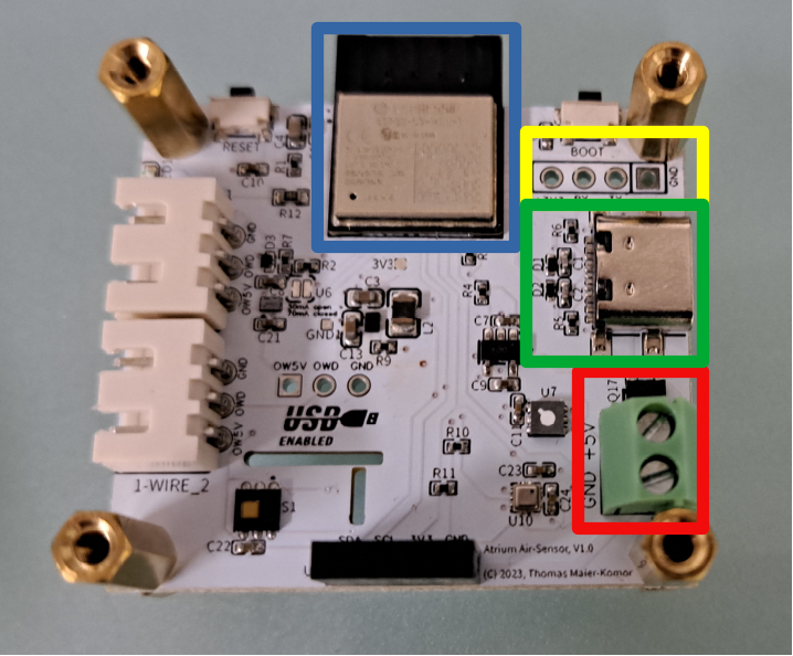
The board below has an ESP32-C3 (blue), an USB-C connector (green), auxiliary power input (red), and an unpopulated header for fall-back serial communication (yellow).
The reason for integrating USB in maker projects is that the ESP32-C3/S3 family of controller supports flashing and serial console via USB, and power-supply comes in as a bonus using the same cable. Additionally, the form factor of a USB port is much smaller than the combination of a barrel-connector for power and a DB-9 connector for RS232.
So this can avoid a whole bunch of cables and wiring complexity and PCB space for the RS232 transceiver. It also makes the setup less prone to errors and easier to use. But the integration of USB has its own complexity and came with some surprises for me, regarding what needs to be done.
Here I want to share some experience, and give a starting point for other makers, who want to dive into this topic of adding USB to their projects.
There are a couple of points to think about when adding USB to an ESP32-C3 or ESP32-S3 based project, which both have native USB support.
The first question that needs to be answered is what kind of connector to place on the board. I decided for USB-C, as the orientation doesn't matter when plugging in. Unfortunately, it turned out that USB-C connectors are different and more complex regarding integration than the micro-USB connectors.
Therefore, let's first discuss the micro USB connector, and then look at the differences and specific topics of the USB-C, after clarifying the basic requirements that are common to all connectors.
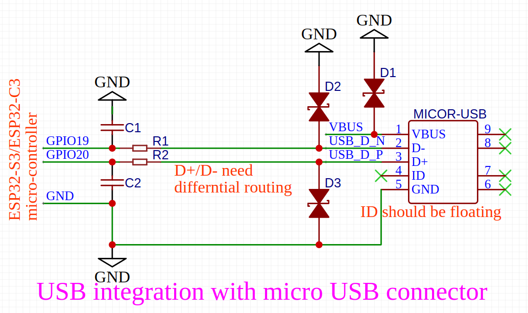
The setup for a micro USB connector is most simple, and only has one pin that is specific to this connector. Below is the schematics for connecting a micro-controller to a micro-USB connector. For the ESP32-S3 and ESP32-C3 you won't need everything, but let's go through it step-by-step, looking at the schematic below that depicts the generic integration of a USB connector to a micro-controller, which can talk the USB protocol via the USB data lines.
-
The first step is simple - of course ground always must be connected to have a common zero volt reference level.
-
Connect Vbus to the input of the voltage regulators or buck converters that supply and stabilize all necessary voltages needed in your system.
-
Adjust the differential impedance of the USB data bus and micro-controller, to be within the required 90 Ohms +/-15%, as required by the USB 2.0 specification. This is done by choosing the correct values for R1 and R2 and placing them close to the micro-controller.
-
Block noise coming from the micro-controller. This is achieved by adding C1 and C2 closely to the micro-controller, with the correct value.
-
Add additional protection measures against transient voltage surges (TVS) on the Vbus and D+/D- lines (TVS diodes D1, D2, and D3 here).
-
Route the differential data lines D+ and D- in parallel with appropriate parameters to adhere to the 90 Ohm differential impedance that is required for USB communication.
-
Leave the ID pin floating. This is specific to the micro USB connector, and the ID pin is only needed for OTG. I.e. it has no relevance here.
Step 1 is straight forward. Adding a ground plane is preferable, or at least having the second layer being mostly a ground layer with well designed return paths.
Step 2 will be part of the typical power supply design. I.e. figure out, which voltages and amps you need, select appropriate bucks or LDOs, and add some decoupling capacitors for Vbus, based on what the power supply devices need. For ESP32-C3 and ESP32-S3 modules you only need 3.3V; chip integration is different and beyond the scope of this article.
Step 3 requires figuring out the correct values for R1 and R2, because the overall impedance of the bus also depends on the device connected to the bus. For the ESP32-C3 and ESP32-S3 it was a bit difficult to figure out what the correct values are, because I haven't found anything in their data-sheets and technical reference manuals. The hardware design guidelines just point out that the RC circuit should be placed close to the micro-controller, but does not talk about values for R and C. But the web page on hardware design guidelines for the ESP32-S3 mentions that R should be populated as 0 Ohm and the capacitor should be left unpopulated.
So, for ESP32-C3 and ESP32-S3 the given value is 0 Ohm - i.e. the resistors can be omitted for these controllers. If you have a different controller or you want to spend the space in case you need to adjust the impedance with a different resistor, be sure to place the termination resistors close to the micro-controller. For other micro-controllers you should be able to find the appropriate values for R1 and R2 in the data-sheet of the relevant device.
Step 4 you should just consider if you want to spend the space for unpopulated C1 and C2. They are really not needed for ESP32-C3 and ESP32-S3, and they should be placed closely to the chip driving the USB bus. Having this footprint reserved can only help you, if you have the tools to figure out that some kind of capacitor for noise filtering is needed, and that is probably only the case if you plan to perform EMI tests etc.. For my maker projects, I just omit these footprints and things works fine.
In case you consider adding capacitors, keep in mind that their value should be less than 50pF per line, according to recommendations from Intel.
Step 5 requires choosing appropriate TVS diodes. There are many kinds available, and you can use different ones for Vbus and the data-lines and choose between individuals and packs of multiple diodes. More on that below.
Step 6 connects D- and D+ to the relevant pins of the micro-controller for USB communication. Be sure to perform a differential routing with appropriate parameters as described below.
Step 7 leaves the ID pin unconnected and floating, as this is used for OTG only and is not discussed any further here.
As written above, the Espressif schematics include zero Ohm termination resistors and unpopulated capacitors for noise decoupling on the D+ and D- lines.
Be aware that the filter should be placed close to the micro-controller to eliminate the high frequency noise as early as possible before it can be radiated to the outside. Unfortunately, the documentation and schematics are a bit misleading as the filter is depicted along with the connector. So you could assume that it should be placed there, but this is actually not the case.
Silicon Labs recommends to add 15 Ohm serial resistors to the USB data lines close to the EFM32 micro-controller. Their application note AN0046 also point out that these resistors are used as terminators for the USB bus. Unfortunately, the Espressif documentation is less clear on that point. But as written above, the hardware guidelines web page points out that R should be zero Ohm, and C can be left out completely.
External interfaces always yield the risk that a high voltage spike could be introduced via the port to the micro-controller and kill its internal circuits. Therefore, adding special TVS (transient voltage surge) diodes is highly recommended to make sure that high voltage spikes are filtered out before they can travel to the micro-controller.
Therefore, TVS diodes are highly recommended to protect the micro-controller and other sensitive parts on your PCB. You can choose between individual diodes or bigger parts that include multiple devices. Anyway, place the TVS diode close to the USB connector.
I found the following ones that I have used and plan to reuse:
- ESD401 from TI: a device for a single data line. It works well for micro-USB connectors (see layout proposal from the data-sheet below). I also use it for 1-wire busses.

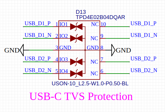
- TPD4E02B04 from TI: this device has 4 diodes and traces can be routed underneath the device without creating stubs. This one is great for USB-C as it can cover data and CC lines with a single device, if you connect the data lines together and only use a single set of data lines. The JLCPCB part number is C106794. Below is the schematics for using this part.
- ESD441 from TI: this one is for Vbus, but it is unfortunately not available at JLCPCB.
There is also a cheap alternative, with 5 diodes in a single package. The device is called SMF05CT1G and its JLCPCB part number is C15879. I used this device for my first design with a USB port, which resulted in stubs in the USB traces on a 2 layer board. I never had problems with the USB full-speed connections on that board. So don't worry too much about signal routing for full-speed USB. Nevertheless, I would not recommend this device, as it does not allow nice routing, as the TPD4E02B04 does.
Additionally, Texas Instruments recommends to add 10nF capacitors to the 4 Vbus lines close to the USB-C connector for USB-PD. There seem to some USB-PD power supplies available that apply 20V to Vbus even when not connected. This behavior does not conform to the standard and can cause damages while connecting. For compliant USB-PD chargers and regular USB chargers this does not seem to be necessary.
The data lines must be routed in parallel, and there must be no stubs on these PCB traces, due to the high frequency of the USB signal on the bus. Additionally, the ESP has only one pair of USB data lines, but there are two pairs on the USB-C connector, which is discussed below.
Routing the data traces from the connector to the micro-controller is the most important task. To do this, I recommend following steps:
- Place the USB connector and the micro-controller as close as possible together, to make routing easier.
- Plan for a keep-out zone around the traces. I.e. do not place any other parts close to these traces, except those explicitly required (see below).
- Place the USB traces on the top layer with a dedicated ground layer below it. For a 2 layer board make sure that the ground area below the traces is reaching well around the USB traces so that there will be no impedance changes for the signal traveling along the USB traces.
- Calculate the necessary trace width and gap between the traces using a trace calculation tool with the parameters of the boards you intend to use for the required differential impedance of 90 Ohms.
- Route the traces in parallel, avoiding any angles bigger than 45 degrees, and make sure the trace lengths match up as close as possible.
- Make sure that any high frequency signal such as SPI or I2C clocks are not routed anywhere close to the USB data lines.
Regarding point 4, the data lines of the USB bus must be routed with a differential impedance of 90 Ohm. The width of the traces and the clearance in between must be calculated based on the copper thickness of the relevant PCB layer. So this depends on the PCB manufacturer and the specific PCB variant selected for the board.
The PCB manufacturer will tell you the thickness of the copper on every layer, and they usually also provide a tool for calculating the differential impedance of a given set of thickness, trace width, and gab between both traces. JLCPCB also has such a tool, which can be found here.
Regarding point 5, to route the traces in parallel, EasyEDA has built-in support for doing this. First you need the parameters for differential routing in the Design Rule section. You should add a specific rule for USB pairs and set the track width, clearance, via diameter, and via drill diameter parameters there.
After that you need to select the pair of signal, which must have a common name
at the beginning and different endings beginning with an underscore character
(e.g. USB_D1_N, USB_D1_P). You can start routing a differential pair, named
appropriately, by selecting Differential Pair Routing in the Route menu.
When using an USB-C connector, some more things must be taken into account, and decisions must be made. These are:
- Set the role of the USB-C port.
- Choose a variant for handling flipped connections: 2a) Short both data-pairs together. 2b) Handle flipped connections correctly using CC read-back and a data-line MUX.
For USB-C, the role must be configured regarding the style of connection. Valid roles are:
- upstream facing port (UFP)
- downstream facing port (DFP)
- dual role port (DRP)
Embedded systems that want to draw power via USB-C, need a UFP port. The DFP role is intended for devices that deliver power to the attached devices. The dual role port (DRP) is the special case, which enables to switch the role between upstream facing and downstream facing based on the attached device and the power situation, which requires support from software. Therefore, implementing DRP is much more complex than UFP and is not discussed here any further.
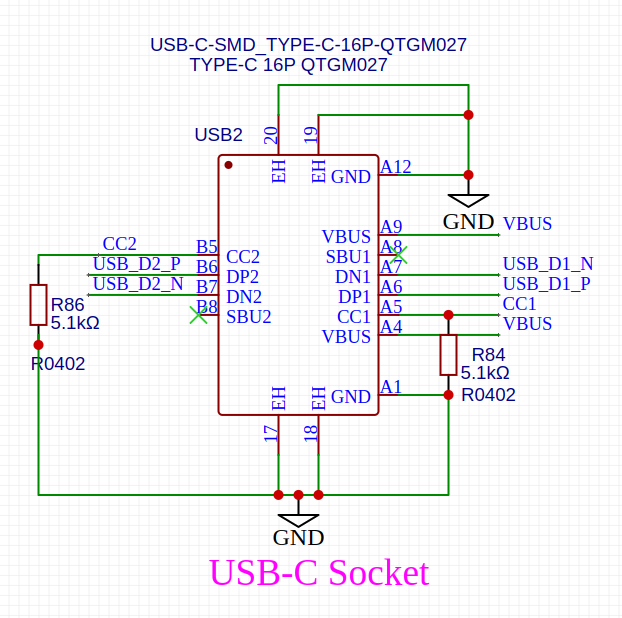
Luckily, configuring a port as UFP is simple. You just need to attach 5k1 pull-down resistors to the CC1 and CC2 lines, and that's it. If you route the CC1/CC2 lines to ADC capable pins of the ESP32-S2/S3/C3, you can use the Atrium USB driver to determine the cable orientation and the current limits signaled via CCx-resistors of the downstream facing port.
The D-channel of the USB cable exists only once, which requires that the PCB must deal with flipped USB connectors so that both cable orientations end up to be connected to the micro-controller based on the way the plug sits in the connector.
Therefore, you have 3 options:
- Connect only one pair of data line pins of the USB-C socket to the micro-controller.
- Short the DP1/DP2 and DN1/DN2 pins directly at the USB-C socket together.
- Place a USB data-line MUX (e.g. T3USB221) on the board and connect both pairs from the connector to the selectable side of the MUX and the other side to the micro-controller and use a GPIO to switch to the correct DN/DP pair based on the information provided via the CCx lines.
The trade-offs of these decisions are as follows:
- If you only connect one pair, the cable orientation will matter if you want to communicate with the micro-controller. If you just want to use that connection for uploading the firmware, this might be OK, but may also cause confusion, if you don't get a connection and don't realize that the data-bus has no connection due to a flipped plug.
- If you short the DNx and DPx pins directly at the connector, you will sacrifice signal quality, due the stubs you are creating. I have done this (even on a 2 layer board), and it worked without any issues, as the ESP32 family only runs with full speed (i.e. 12Mb/s). ) Placing an USB MUX on the board is the correct solution, but of course comes with additional BOM costs. Furthermore, a MUX will not be switched to the correct pins by the flashing software on the device, as it is unaware of the CCx lines, and how to operate the MUX.
Solution 1: This is the easiest approach, but the outcome of this approach that the device will not be able to perform any USB communication if the plug is attached in the incorrect orientation. Forget about this approach, it just causes headaches if you forget or don't know, that a flipped plug will not work...
Solution 2: The pragmatic way to solve this problem is to connect both
endpoints of the D-channel connectors together on the board with a PCB trace.
This actually works for the slower speeds of USB (i.e. it is good enough for
ESP32-C3/S3): i.e. connect USB_D1_N to USB_D2_N, and USB_D1_P to
USB_D2_P.
This makes sure both pairs are connected to the micro-controller, but creates a small stub at the unconnected pair, which will decrease signal integrity. But this is not a problem for full-speed USB communication (i.e. 12Mb/s), and therefore I recommend this approach, as it worked for me on several boards.
Solution 3: This is hard, expensive, correct, but probably also over-engineered way to solve the problem. It requires that software determines the plug orientation and set the USB MUX accordingly, to make sure the correct data pair is routed to the micro-controller.
Below is a schematic of a T3USB221 USB MUX. The enable and select lines should be pulled down to assume a default level that enables the USB and connects the uC to the data lines of the unflipped plug. As an alternative, you can connect those pins to GPIO45 and GPIO46 of the ESP32-S3, which have pull-downs enabled during power-up. Like this you can omit the 10k resistors.

Anyway, after power-up the CCx lines must be evaluated to determine the orientation of the plug and switch over to the other pair of data lines, in case the plug is flipped.
Of course this kind of software magic can only work if the firmware already has been flashed to the target. I.e. the default MUX setting must match the plug orientation to be able to perform flashing of the device. So this is also a disadvantage over solution #2.
Therefore, I rather recommend solution 2.
If you plan to add an additional power source, you should add an 1N5819 diode between Vbus and your 5V rail to make sure the USB bus only takes over when the 5V rail has no power source of its own. Additionally, it makes sure that the Vbus does not get powered by two sources in parallel, which for sure would cause problems.
Below, you can see the 2D plot of the photo depicted above. As you can see, I wrongly placed the noise cancelling capacitors (22pF in that case) close to the connector. But the are well below the limit of the Intel recommendation of 50pF.

Furthermore, you can see that the traces are routed in parallel without any sharp angles, and the distance between the connector and the micro-controller is pretty small. The data-lines are shorted directly at the connector. The CC resistors for configuring this port as UFP, are placed close to the connector (not needed), and there are two dedicated diodes (D1,D2) for TVS protection. The diode for protecting Vbus against the auxiliary power input is missing here, which was actually a conscious decision, because the application is either power by AUX or attached to USB for development.
This USB setup on this board works without any issues.
Taking everything into account, I recommend the following set-up for the ESP32-C3,S2,S3 devices:
- Select an USB-C connector of your choice.
- For USB-C connectors, short the D1+/D2+ and the D1-/D2- data-lines so that the orientation of the plug does not matter.
- Omit the resistors for impedance adoption.
- Omit the capacitors for noise filtering.
- Add a TPD4E02B04 for TVS protection and route the data-pair and CC lines below it.
- If you have free ADC inputs, route the CC1/CC2 lines to ADC capable inputs, then you can determine the maximum allowed current and the plug orientation using the Atrium driver for the CCx lines.
This approach has low BOM costs, the versatility of USB-C, TVS protection, and low integration complexity (no additional software needed).
Finally, just give it a try. The fast speed mode of USB seems to be quite forgiving when it comes to suboptimal tracing of the data lines. This is in every aspect better as the traditional dedicated power plus JTAG adapter plus serial console approach.