BBB_cci_gemm
The GEMM IP for Intel FPGA is based on 2-D systolic array architecture. The GEMM Core consists of processing elements (PE) laid out in a two dimensional array. Each PE is responsible for doing a dot product of two vectors. Note that the number of elements in these vectors depends on the data type being used in the GEMM. For FP-32 mode, each PE is responsible for doing the dot product of two 8 element vectors. For INT-16 mode, each PE is responsible for doing the dot product of two 16 element vectors. For INT-8 mode, each PE is responsible for doing the dot product of two 32 element vectors. Along with performing the dot product, the PEs are also responsible for propagating the vectors to its neighbors (both above and to the right). In all, there are 160 PEs organized in 10 rows and 16 columns.
Figure 1 shows the various building blocks that are connected to the GEMM IP. The GEMM IP is directly connected to the MPF. The MPF is a basic building block that provides the virtual to physical address translation services for the AFU using a TLB in the hardware. The MPF is connected to the CCI-P interface. The Async FIFO shim is an optional block that can be used between the MPF and CCI-P interface in order to allow the GEMM IP to run at a lower frequency than that of the CCI-P interface.
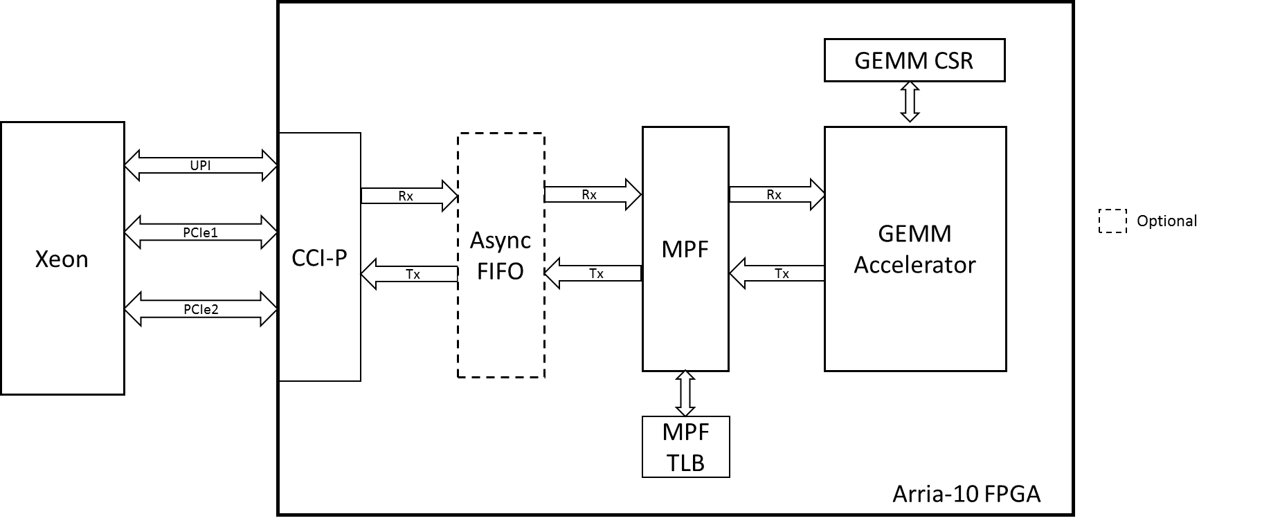
Figure 1: GEMM IP with CCI-P and MPF
Figure 2 shows the systolic array architecture of the GEMM IP. The elements of matrix A are sent in chunks to the row feeders and elements of matrix B are sent in chunks to the column feeders. All the PEs are arranged in a 2-D array of 10x16, resulting in 160 PEs. Note that the chunk size fed into the PEs for a given matrix multiplication is selected based on control and status registers (CSRs).
The chunk size used for matrix A and matrix B can be different. However, the chunk size for all PEs fed from matrix A is the same, and the chunk size for all PEs fed from matrix B is the same. Because of this, each PE produces an equal sized section of the final result matrix. The specific size of this section (as determined by the CSRs) is equal to the chunk size of A by the chunk size of B. For example, if the chunk size of A is set to 8 and the chunk size of B is set to 10, then each PE would calculate an 8x10 section of the final result matrix.
Note that there are some restrictions on the allowed chunk sizes. The minimum allowed chunk size for matrix A is 2, the minimum allowed chunk size for matrix B is 5, and the maximum allowed chunk size for both matrices is 32. Furthermore, the chunk size of A multiplied by the chunk size of B must be greater than 50. This means that if the chunk size of A is set to 5, the chunk size of B cannot be set to 10 (but could be set to 11).
Lastly, since there are 10 rows of PEs and the minimum chunk size of A is 2, the minimum size for the number of rows in matrix A is 20 (2 times 10 rows). Similarly, since we have 16 columns of PEs and the minimum chunk size of B is 5, the minimum size for the number of columns in matrix B is 80 (5 times 16 columns). However, note that due to the limitations of the chunk size values mentioned before, it is not possible to use the minimum row size of A in conjunction with the minimum column size of B.

Figure 2: Systolic Array of PEs
The functionality of the GEMM IP is managed through the use of control and status registers (CSRs) that are exposed through the MMIO interface of the CCI-P.
Table 1: GEMM CSR and its description
| CSR Name | Offset | Size | CCI-P Mandatory | Description |
|---|---|---|---|---|
| CSR_AFH_DFH_BASE | 0x000 | 64 bits | Yes | Device feature header |
| CSR_AFH_ID_L | 0x008 | 64 bits | Yes | Lower 64 bits of the GEMM GUID |
| CSR_AFH_ID_H | 0x010 | 64 bits | Yes | Upper 64 bits of GEMM GUID |
| CSR_AFU_DSM_BASE | 0x100 | 64 bits | GEMM Specific | AFU DSM base address |
| CSR_VERSION | 0x110 | 64 bits | GEMM Specific | Systolic GEMM Version |
| CSR_CTL | 0x118 | 64 bits | GEMM Specific | Control CSR for controlling operation of the GEMM IP |
| CSR_CFG | 0x120 | 64 bits | GEMM Specific | Configures the write type and read type used through CCI-P |
| CSR_SRC_ADDR_A | 0x128 | 64 bits | GEMM Specific | Pointer to the base address of matrix A |
| CSR_SRC_ADDR_B | 0x130 | 64 bits | GEMM Specific | Pointer to the base address of matrix B |
| CSR_DST_ADDR_C | 0x138 | 64 bits | GEMM Specific | Pointer to the base address of matrix C |
| CSR_NUM_BLOCKS | 0x140 | 64 bits | GEMM Specific | Number of blocks in a workload |
| CSR_NUM_PARTS_A | 0x148 | 64 bits | GEMM Specific | Number of partitions in matrix A |
| CSR_NUM_PARTS_B | 0x150 | 64 bits | GEMM Specific | Number of partitions in matrix B |
| CSR_NUM_PARTS_C | 0x158 | 64 bits | GEMM Specific | Number of partitions in matrix C |
| CSR_NUM_ROWS_X_NUM_BLOCKS | 0x160 | 64 bits | GEMM Specific | Software must write into this CSR the product of the number of rows (10) in the GEMM core and the number of blocks represented by CSR_NUM_BLOCKS |
| CSR_NUM_COL_X_NUM_BLOCKS | 0x168 | 64 bits | GEMM Specific | Software must write into this CSR the product of number of columns (16) in the GEMM core and number of blocks represented by CSR_NUM_BLOCKS |
| CSR_NUM_CACHE_LINES_C | 0x170 | 64 bits | GEMM Specific | Software must write into this CSR the number of cache lines that comprise matrix C. This value is used by the HW to check the condition for GEMM computation complete. |
| CSR_CHUNK_SIZE_A | 0x178 | 64 bits | GEMM Specific | Number of vectors contained within a single chunk of matrix A |
| CSR_CHUNK_SIZE_B | 0x180 | 64 bits | GEMM Specific | Number of vectors contained within a single chunk of matrix B |
| CSR_GROUP_SIZE | 0x188 | 64 bits | GEMM Specific | Number of chunks contained within a single group |
Table 2: CSR_AFH_DFH_BASE description
| Bit | Attribute | Default | Description |
|---|---|---|---|
| 63:60 | Read only | 0x1 | Type: AFU |
| 59:52 | RSVD | 0x0 | Reserved |
| 51:48 | Read only | 0x0 | AFU Minor version |
| 47:41 | RSVD | 0x0 | Reserved |
| 40 | Read only | NA | End of list 1’b0 - There is another feature header beyond this 1’b1 - This is the last feature for this AFU |
| 39:16 | Read only | 0x0 | Byte offset to the Next device feature Header. For MPF, the byte offset address is 0x1000 |
| 15:12 | Read only | NA | AFU Major version |
| 11:0 | Read only | 0x070 | CCI-P version |
The AFU GUID is the architectural interface/contract that the AFU makes with the SW. The same GEMM IP supports 3 modes (each with its own bitstream).
-
GEMM FP-32: 64f6fa35-6025-4e72-ad92-15c3-a431-73a9
-
GEMM INT-16: 311791dc-97e9-4783-87b7-0d33-b119-0613
-
GEMM INT-8: da52758f-3f2a-45c1-89de-7762-7064-30ea
CSR_AFH_ID_L stores the lower 64 bit of the GEMM FP-32 AFUID
Table 3: CSR_AFH_ID_L description for GEMM FP-32
| Bits | Attribute | Default | Description |
|---|---|---|---|
| 63:0 | Read only | 0 | 64’h AD92_15C3_A431_73A9 |
CSR_AFH_ID_H stores the higher 64 bit of GEMM FP-32 AFUID
Table 4: CSR_AFH_ID_H description for GEMM FP-32
| Bits | Attribute | Default | Description |
|---|---|---|---|
| 63:0 | Read only | 0 | 64’h64F6_FA35_6025_4E72 |
CSR_AFH_ID_L stores the lower 64 bit of the GEMM INT-16 AFUID
Table 5: CSR_AFH_ID_L description for INT-16
| Bits | Attribute | Default | Description |
|---|---|---|---|
| 63:0 | Read only | 0 | 64'h87B7_0D33_B119_0613 |
CSR_AFH_ID_H stores the higher 64 bit of GEMM INT-16 AFUID
Table 6: CSR_AFH_ID_H description for INT-16
| Bits | Attribute | Default | Description |
|---|---|---|---|
| 63:0 | Read only | 0 | 64'h3117_91DC_97E9_4783 |
CSR_AFH_ID_L stores the lower 64 bit of the GEMM INT-8 AFUID
Table 7: CSR_AFH_ID_L description for INT-8
| Bits | Attribute | Default | Description |
|---|---|---|---|
| 63:0 | Read only | 0 | 64'hDA52_758F_3F2A_45C1 |
CSR_AFH_ID_H stores the higher 64 bit of GEMM INT-8 AFUID
Table 8: CSR_AFH_ID_H description for INT-8
| Bits | Attribute | Default | Description |
|---|---|---|---|
| 63:0 | Read only | 0 | 64'h89DE_7762_7064_30EA |
CSR_AFU_DSM_BASE is a 64-bit register that stores the virtual address of the DSM address space. The GEMM uses the DSM for FPGA to CPU signaling. The GEMM IP always writes to a specific address in the DSM address space and the software should poll on this address to check if a GEMM computation is complete.
The address of the status complete flag can be found using
*StatusAddr = (CSR_AFU_DSM_BASE) + 0x40.
StatusAddr is a 32-bit CSR in the DSM address space. The GEMM software should poll bit 0 within this CSR to determine when a GEMM computation is complete.
Table 9: StatusAddr CSR (within DSM) description
| Bits | Attribute | Default | Description |
|---|---|---|---|
| StatusAddr[0] | RW | 0 | 0: GEMM compute not complete 1: GEMM compute complete |
The software must reset the StatusAddr[0] before the start of the next execution.
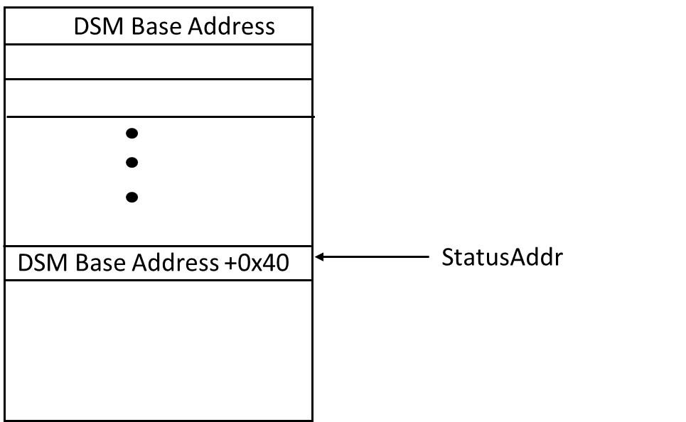
Figure 3: StatusAddr location in DSM Address Space
Software can read the CSR_VERSION register to get the GEMM version.
Table 10: CSR_VERSION description
| Bits | Attribute | Description |
|---|---|---|
| CSR_VERSION[63:0] | RO | [63:48] – RSVD [47:32] – Major Revision [31:16] – Minor Revision [15:0] – Patch Revision |
CSR_CTL is used to control when the GEMM IP starts computing. Under normal operations, the GEMM IP will complete and stop on its own. In the rare case that a computation must be ended early, the CSR_CTL allows for a way to force the GEMM IP to stop computing.
Table 11: CSR_CTL description
| Bits | Attribute | Default | Description |
|---|---|---|---|
| CSR_CTL[1:0] | RW | 00 | 00 – RSVD 01 – GEMM Start 10 – GEMM Stop 11 – RSVD |
CSR_CFG is used to configure the channels and types of memory requests that occur during computation of the GEMM.
Table 12: CSR_CFG description
| Bits | Attribute | Default | Description |
|---|---|---|---|
| CSR_CFG[17:16] | RW | 00 | Channel Type Select 00 – VA 01 – VL0 10 – VH0 11 – VH1 |
| CSR_CFG[11:8] | RW | 0000 | Read Type Select 0000 - eREQ_RDLINE_I 0001 - eREQ_RDLINE_S Others - RSVD |
| CSR_CTL[3:0] | RW | 0000 | Write Type Select 0000 – eREQ_WRLINE_I 0001 – eREQ_WRLINE_M Others - RSVD |
The software writes the memory pointer of matrix A into this CSR. The GEMM IP uses this address to calculate the offsets to read matrix A data.
Table 13: CSR_SRC_ADDR_A description
| Bits | Attribute | Description |
|---|---|---|
| CSR_SRC_ADDR_A[63:0] | RW | [63:0] - Memory pointer to matrix A |
The software writes the memory pointer of matrix B into this CSR. The GEMM IP uses this address to calculate the offsets to read the matrix B data.
Table 14: CSR_SRC_ADDR_B description
| Bits | Attribute | Description |
|---|---|---|
| CSR_SRC_ADDR_B[63:0] | RW | [63:0] - Memory pointer to matrix B |
The software writes the memory pointer of matrix C into this CSR. The GEMM IP uses this address to calculate the offsets to write the matrix C data.
Table 15: CSR_SRC_ADDR_C description
| Bits | Attribute | Description |
|---|---|---|
| CSR_SRC_ADDR_C[63:0] | RW | [63:0] - Memory pointer to matrix C |
The CSR_NUM_BLOCKS specifies the number of blocks in a workload that are processed across the inner (a.k.a common) dimension during the matrix multiplication.
Table 16: CSR_NUM_BLOCKS description
| Bits | Attribute | Description |
|---|---|---|
| CSR_NUM_BLOCKS[63:0] | RW | [63:0] - Number of blocks in a workload |
The number of blocks in a workload (i.e. the value that software needs to write into this register) is defined by the following equation:
k / (ELEMENTS_PER_VECTOR * CSR_GROUP_SIZE)
| Equation Parameters | Description |
|---|---|
| k | The number of columns in matrix A (or the number of rows in matrix B) |
| ELEMENTS_PER_VECTOR | Equals 8 in FP-32 Equals 32 in INT-8 |
| CSR_GROUP_SIZE | Value from another CSR |
Note that the value in this CSR needs to be programmed by the software before the start of GEMM computation.
The CSR_NUM_PARTS_A specifies the number of parts that matrix A can be partitioned and processed across the outer dimension of matrix A (i.e. the rows of matrix A) during the matrix multiplication.
Table 17: CSR_NUM_PARTS_A description
| Bits | Attribute | Description |
|---|---|---|
| CSR_NUM_PARTS_A[63:0] | RW | [63:0] - Number of partitions in matrix A |
The number of partitions in matrix A (i.e. the value that software needs to write into this register) is defined by the following equation:
m / (10 * CSR_CHUNK_SIZE\ A)
| Equation Parameters | Description |
|---|---|
| m | The number of rows in matrix A |
| CSR_CHUNK_SIZE_A | Value from another CSR |
Note that the value in this CSR needs to be programmed by the software before the start of GEMM computation.
The CSR_NUM_PARTS_B specifies the number of parts that matrix B can be partitioned and processed across the outer dimension of matrix B (i.e. the columns of matrix B) during the matrix multiplication.
Table 18: CSR_NUM_PARTS_B description
| Bits | Attribute | Description |
|---|---|---|
| CSR_NUM_PARTS_B[63:0] | RW | [63:0] – Number of partitions in matrix B |
The number of partitions in matrix B (i.e. the value that software needs to write into this register) is defined by the following equation:
n / (16 * CSR_CHUNK_SIZE_B)
| Equation Parameters | Description |
|---|---|
| n | The number of columns in matrix B |
| CSR_CHUNK_SIZE_B | Value from another CSR |
Note that the value in this CSR needs to be programmed by the software before the start of GEMM computation.
The CSR_NUM_PARTS_C specifies the number of blocks in the matrix C result.
Table 19: CSR_NUM_PARTS_C description
| Bits | Attribute | Description |
|---|---|---|
| CSR_NUM_PARTS_C[63:0] | RW | [63:0] – Number of partitions in matrix C |
The number of blocks in matrix C (i.e. the value that software needs to write into this register) is equal to CSR_NUM_PARTS_A*CSR_NUM_PARTS_B.
Note that the value in this CSR needs to be programmed by the software before the start of GEMM computation.
This CSR must be written by software, and it should contain the product of the number of rows (10) in the GEMM core and number of blocks represented by CSR_NUM_BLOCKS.
Table 20: CSR_NUM_ROWS_X_NUM_BLOCKS description
| Bits | Attribute | Description |
|---|---|---|
| CSR_NUM_ROWS_X_NUM_BLOCKS[63:0] | RW | [63:0] - 10 * CSR_NUM_BLOCKS |
This CSR must be written by software, and it should contain the product of the number of columns (16) in the GEMM core and number of blocks represented by CSR_NUM_BLOCKS.
Table 21: CSR_NUM_COL_X_NUM_BLOCKS description
| Bits | Attribute | Description |
|---|---|---|
| CSR_NUM_COL_X_NUM_BLOCKS[63:0] | RW | [63:0] - 16 * CSR_NUM_BLOCKS |
This CSR must be written by software, and it should contain the number of cache lines that must be written to complete the computation of matrix C. This value is used by the HW to check for the condition that the GEMM computation has completed.
Table 22: CSR_NUM_CACHE_LINES_C description
| Bits | Attribute | Description |
|---|---|---|
| CSR_NUM_CACHE_LINES_C[63:0] | RW | [63:0] - Number of cache line writes needed for matrix C to finish computation |
The CSR_CHUNK_SIZE_A specifies the number of vectors that are contained in a chunk of matrix A. Because this CSR controls the number of vectors that are sent to the matrix A side of the PEs, it also means that this CSR directly controls the number of rows that are contained within a block of matrix A. In other words, this CSR allows for dynamically selecting the outer dimension of matrix A that is used for the matrix multiplication. The number of elements used for the matrix multiplication in the outer dimension of matrix A is defined by the following equation:
Rows in a block of matrix A = 10 * CSR_CHUNK_SIZE_A
Table 23: CSR_CHUNK_SIZE_A description
| Bits | Attribute | Description |
|---|---|---|
| CSR_CHUNK_SIZE_A [63:0] | RW | [63:0] - Number of vectors in a chunk of matrix A |
It should be noted that the number of vectors in a chunk of matrix A (along with the number of vectors in a chunk of matrix B) is what determines the size of the matrix C section that is calculated within each PE. This specific size that is calculated within each PE is equal to CSR_CHUNK_SIZE_A x CSR_CHUNK_SIZE_B. As an example, if CSR_CHUNK_SIZE_A is set to 10 and CSR_CHUNK_SIZE_B is set to 11, then each PE calculates a 10x11 section of the matrix C result.
It should be noted that there are some restrictions on the values that can be used in CSR_CHUNK_SIZE_A. The minimum allowed value is 2, the maximum allowed value is 32, and the value of CSR_CHUNK_SIZE_A*CSR_CHUNK_SIZE_B must be greater than 50.
Note that the value in this CSR needs to be programmed by the software before the start of GEMM computation.
The CSR_CHUNK_SIZE_B specifies the number of vectors that are contained in a chunk of matrix B. Because this CSR controls the number of vectors that are sent to the matrix B side of the PEs, it also means that this CSR directly controls the number of columns that are contained within a block of matrix B. In other words, this CSR allows for dynamically selecting the outer dimension of matrix B that is used for the matrix multiplication. The number of elements used for the matrix multiplication in the outer dimension of matrix B is defined by the following equation:
Columns in a block of matrix B = 16 * CSR_CHUNK_SIZE_B
Table 24: CSR_CHUNK_SIZE_B description
| Bits | Attribute | Description |
|---|---|---|
| CSR_CHUNK_SIZE_B [63:0] | RW | [63:0] - Number of vectors in a chunk of matrix B |
It should be noted that the number of vectors in a chunk of matrix B (along with the number of vectors in a chunk of matrix A) is what determines the size of the matrix C section that is calculated within each PE. This specific size that is calculated within each PE is equal to CSR_CHUNK_SIZE_A x CSR_CHUNK_SIZE_B. As an example, if CSR_CHUNK_SIZE_A is set to 10 and CSR_CHUNK_SIZE_B is set to 11, then each PE calculates a 10x11 section of the matrix C result.
It should be noted that there are some restrictions on the values that can be used in CSR_CHUNK_SIZE_B. The minimum allowed value is 5, the maximum allowed value is 32, and the value of CSR_CHUNK_SIZE_A*CSR_CHUNK_SIZE_B must be greater than 50.
Note that the value in this CSR needs to be programmed by the software before the start of GEMM computation.
The CSR_GROUP_SIZE specifies the number of chunks that are sent to both the matrix A side and the matrix B side of the PEs before the matrix multiplication calculations move on to the next block. Because this CSR controls the number of chunks (and thus vectors) that are sent to both the matrix A and the matrix B side of the PEs, it also means that this CSR directly controls the number of elements that are contained within the common dimension of a block of matrix A and matrix B. In other words, this CSR allows for dynamically selecting the inner (a.k.a. common) dimension used for the matrix multiplication. The number of elements used for the matrix multiplication in the common dimension is defined by the following equation:
Common dimension elements in a block of matrix A and B = ELEMENTS_PER_VECTOR * CSR_GROUP_SIZE
Table 25: CSR_GROUP_SIZE description
| Bits | Attribute | Description |
|---|---|---|
| CSR_GROUP_SIZE [63:0] | RW | [63:0] - Number of chunks in a group within matrix A (or matrix B) |
It should be noted that there are some restrictions on the values that can be used in CSR_GROUP_SIZE. The value must be an even number, the minimum allowed value is 2, and the maximum allowed value is 16.
Note that the value in this CSR needs to be programmed by the software before the start of GEMM computation.
Matrix A of dimension m by k is split into block sizes as defined by the below matrix size:
(10 * CSR_CHUNK_SIZE_A) x (ELEMENTS_PER_VECTOR * CSR_GROUP_SIZE)
The best case is to process a matrix A whose m and k dimensions are a multiple of “10*CSR_CHUNK_SIZE_A” and “ELEMENTS_PER_VECTOR*CSR_GROUP_SIZE” respectively. This is often possible due to the ability to choose a CSR_CHUNK_SIZE_A and CS_GROUP_SIZE that best align with the size of matrix A. However, for the cases where the matrices are not multiples of the block sizes, those matrices can be zero padded to the nearest size of m and k that is a multiple of the block size.

Figure 4: Partitioning matrix A into blocks
From the GEMM hardware point of view, everything is a Cache Line (CL) aligned address. Hence, it is important to align the contents of matrix A memory in a CL aligned format as shown in the following figures.

Figure 5: Partition a block of matrix A into Feeders and representing in GEMM format

Figure 6: Partition two blocks of matrix A into Feeders and represent in GEMM format
Figures 7, 8, and 9 show how the matrix A with index A[i][j] is mapped to a cache line for different values of CSR_CHUNK_SIZE_A. Note that the byte field in the following figures indicate the byte index in that cache line, which is 64 bytes in length. So “Byte: 0” is the 0th byte in the cache line and “Byte: 4” is the 4th byte in the cache line.
Also note that these figures assume each element in A is an FP-32 (4 byte) element. In the case that each element is an INT-8 (1 byte) element, then each A[i][j] element in the figures below actually contains four 1-byte elements instead of one 4-byte element.

Figure 7: The matrix A element mapping in Cache Line (CSR_CHUNK_SIZE_A = 32)

Figure 8: The matrix A element mapping in Cache Line (CSR_CHUNK_SIZE_A = 16)

Figure 9: The matrix A element mapping in Cache Line (CSR_CHUNK_SIZE_A = 5)
Matrix B of dimension k by n is split into block sizes as defined by the below matrix size:
(ELEMENTS_PER_VECTOR * CSR_GROUP_SIZE) x (16 * CSR_CHUNK_SIZE_B)
The best case is to process a matrix B whose k and n dimensions are a multiple of “ELEMENTS_PER_VECTOR*CSR_GROUP_SIZE” and “16*CSR_CHUNK_SIZE_B” respectively. This is often possible due to the ability to choose a CSR_CHUNK_SIZE_B and CS_GROUP_SIZE that best align with the size of matrix B. However, for the cases where the matrices are not multiples of the block sizes, those matrices can be zero padded to the nearest size of k and n that is a multiple of the block size.
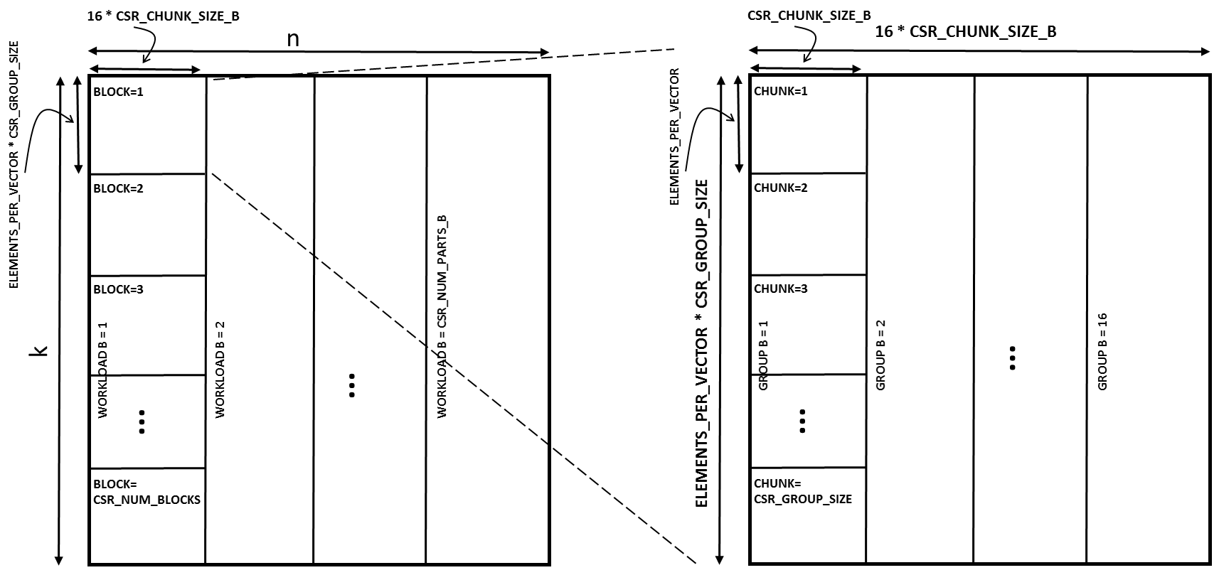
Figure 10: Partitioning matrix B into blocks
From the GEMM hardware point of view, everything is a Cache Line (CL) aligned address. Hence, it is important to align the contents of matrix B memory in a CL aligned format as shown in the following figure.

Figure 11: Partition a block of matrix B into Feeders and represent in GEMM format
Figure 12, 13, and 14 show how the matrix B with index B[i][j] is mapped to a cache line for different values of CSR_CHUNK_SIZE_B. Note that the byte field in the following figures indicate the byte index in that cache line, which is 64 bytes in length. So “Byte: 0” is the 0th byte in the cache line and “Byte: 4” is the 4th byte in the cache line.
Also note that these figures assume each element in B is an FP-32 (4 byte) element. In the case that each element is an INT-8 (1 byte) element, then each B[i][j] element in the figures below actually contains four 1-byte elements instead of one 4-byte element.

Figure 12: The matrix B element mapping in Cache Line (CSR_CHUNK_SIZE_B = 32)

Figure 13: The matrix B element mapping in Cache Line (CSR_CHUNK_SIZE_B = 16)

Figure 14: The matrix B element mapping in Cache Line (CSR_CHUNK_SIZE_B = 5)
The resultant matrix C is organized in the memory with the following format. Each block of matrix C is split into block sizes as defined by the below matrix size:
(10 * CSR_CHUNK_SIZE_A) x (16 * CSR_CHUNK_SIZE_B)
The number of blocks in the matrix C result depends on the values in CSR_NUM_PARTS_A and CSR_NUM_PARTS_B. For example, if CSR_NUM_PARTS_A = 2 and CSR_NUM_PARTS_B = 2, then the total number of blocks in matrix C will be 4, with each block consisting of a “10*CSR_CHUNK_SIZE_A” x “16*CSR_CHUNK_SIZE_B” section of the final resultant matrix. The number of cache lines in the resultant blocks of matrix C can be calculated using the below equation:
Cache lines in a block of matrix C = (CSR_CHUNK_SIZE_A * CSR_CHUNK_SIZE_B * 160 * 4) / 64
Each PE in the systolic array produces a “CSR_CHUNK_SIZE_A”x”CSR_CHUNK_SIZE_B” block in the final matrix C result. Some cases using various values for CSR_CHUNK_SIZE_A and CSR_CHUNK_SIZE_B are illustrated in the following figures.

Figure 15: Matrix C cache line order (CSR_CHUNK_SIZE_A = 32 and CSR_CHUNK_SIZE_B = 32)
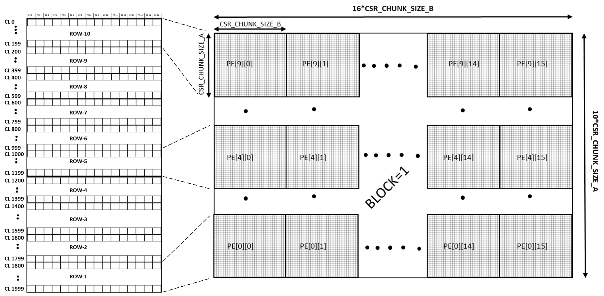
Figure 16: Matrix C cache line order (CSR_CHUNK_SIZE_A = 10 and CSR_CHUNK_SIZE_B = 20)
The “CSR_CHUNK_SIZE_A”x”CSR_CHUNK_SIZE_B” elements from each PE are stored in a linear fashion. When draining the results from the PE, each column PE writes to a fixed location in the cache line. For example, PE[0] writes to the 0th byte in a cache line, PE[1] writes to the 4th byte and so on. This is illustrated in following figures.

Figure 17: Matrix C cache line format (CSR_CHUNK_SIZE_A = 32 and CSR_CHUNK_SIZE_B = 32)
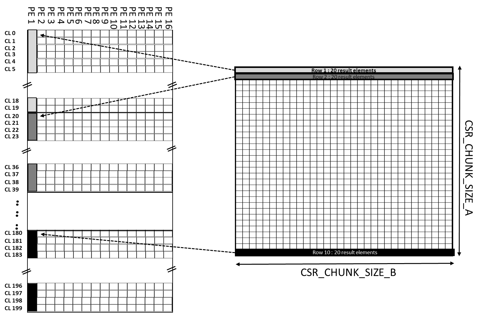
Figure 18: Matrix C cache line format (CSR_CHUNK_SIZE_A = 10 and CSR_CHUNK_SIZE_B = 20)
If matrix A is partitioned in CSR_NUM_PARTS_A blocks and matrix B is partitioned in CSR_NUM_PARTS_B blocks, then the total number of C blocks is the product of CSR_NUM_PARTS_A and CSR_NUM_PARTS_B. For cases where there are more than 1 block of matrix C, the subsequent matrix C blocks are filled in column first format. This is illustrated in the following figures.

Figure 19: Matrix C cache line order for multiple blocks (CSR_CHUNK_SIZE_A = 32 and CSR_CHUNK_SIZE_B = 32)
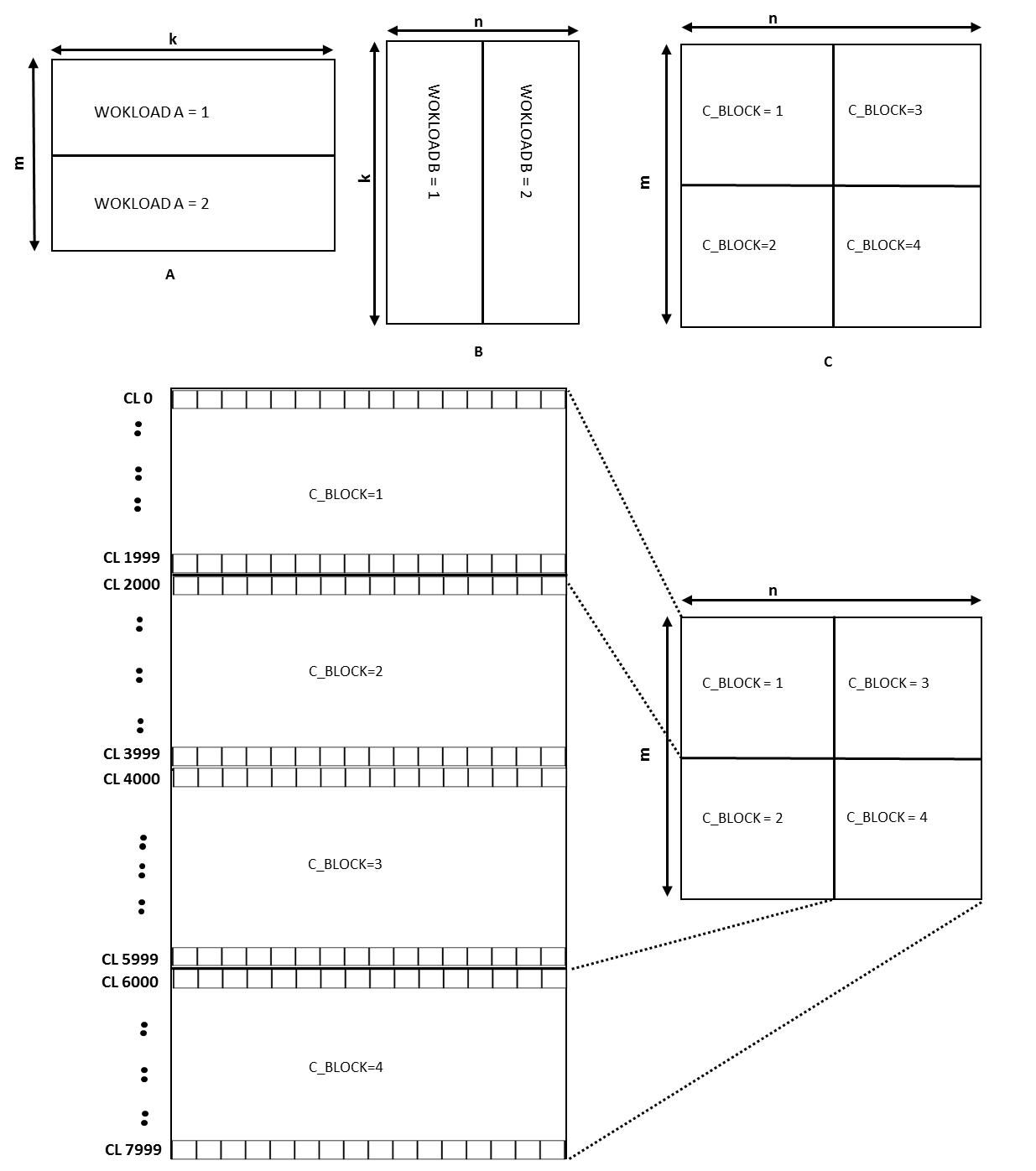
Figure 20: Matrix C cache line order for multiple blocks (CSR_CHUNK_SIZE_A = 10 and CSR_CHUNK_SIZE_B = 20)